Engineering is a unique field as it seamlessly integrates the reliability of science with the uniqueness of self-expression. Its practitioners, particularly those of us who design electronic circuit boards, are both skilled artisans and artists. PCB designers rely on proven principles and technological devices to give ideas a canvas that is transformed into a physical embodiment, bringing those ideas to life.
However, the path from a schematic to a PCB layout to a usable board is bounded. Specifically, your material choices, board dimensions, and other design decisions must fall within the range of capabilities of your CM’s processes and equipment. This means acquiring and following your CM’s DFM and DFA rules and guidelines. Doing so and collaborating with your CM will enable your design intent to be incorporated into the board build process and facilitate efficient PCB design and development that targets the achievement of your performance objectives.
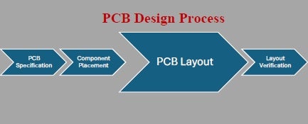
For the best results, the PCB layout design process, which is typically the most complex and time-consuming, must be optimized. Achieving this objective requires a good understanding of the PCB layout design steps and how to maximize the impact of this critical stage on overall circuit board design and development efficiency.
Laying Out Your Circuit Board
A verified schematic is a prerequisite for a good board design. More important is careful consideration and definition of the constraints for your PCB layout. Virtually all PCB layout design packages include default constraint specifications, such as those specified for performance classes 1, 2, and 3 in IPC-6011 General Performance Specification for Printed Boards. These general specifications are important guidelines; however, to ensure the best board by your chosen contract manufacturer (CM), you should acquire and utilize their design for manufacturing (DFM) and design for assembly (DFA) rules and guidelines.
In some cases, you should be able to upload these specifications, which can be extensive. If not, the more advanced PCB design packages typically include a constraint manager that allows you to create and edit constraints. It is essential to follow these rules, which in many cases determine whether or not your board can be built, at least not without redesign. Laying out your board can be divided into four major steps, as described below.
PCB Specification
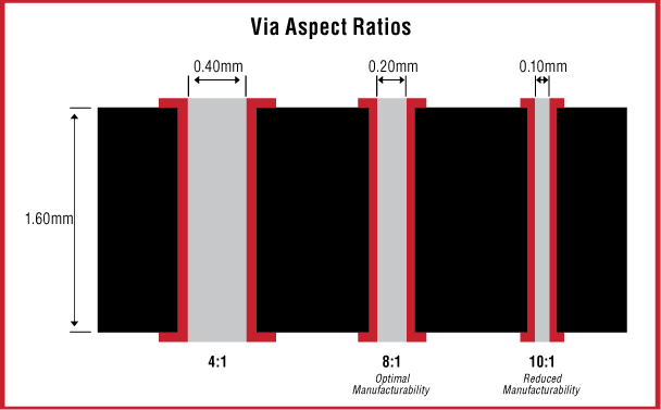
FR-4 is by far the most common board material, although for certain applications, thermal or other requirements necessitate a different material be used. Drilling specs for plated through holes (PTHs) like vias and non-plated through holes (NPTHs) for mounting screws, as well as aspect ratios, as shown below, are also defined during this stage.
For efficient PCB layout design, these and other stackup best practices should be followed.
Placing Components
Just as for schematic generation or capture (another commonly used term for generating the schematic), placing components is an important stage. However, for board layout, there are important regulations to follow, such as component clearance, spacing, and board edge clearance. Other considerations that necessitate you to follow some best practices are listed below.
Following these and other good practices for component placement will help avoid manufacturing problems.
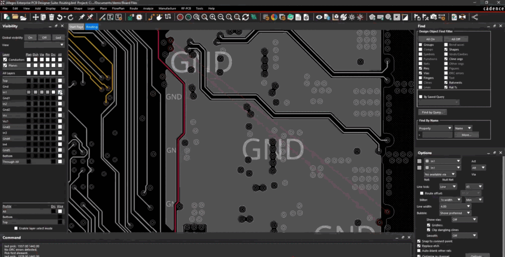
Routing Traces
Although traces connect your board’s components, the process is quite different from creating the nets. In fact, the nets are typically used to create ratlines (guidelines that show what the interconnections should be) that are helpful for manually routing your board. Fortunately, most PCB design tools include some type of auto-routing. These tools may not eliminate all manual routing but can significantly decrease the time required to route your board.
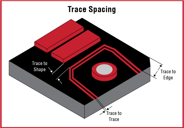
Traces must adhere to certain guidelines, including limits on size and copper thickness given in your CM’s DFM specifications. Additionally, spacing, as defined below, must adhere to standard clearance requirements.
There are other important constraints and considerations that should be included during this stage. Some of these are based on board application or type. For example, when differential signals are used the traces must be identical in length, impedance, and copper weight, and be equidistant from each other.
Layout Verification
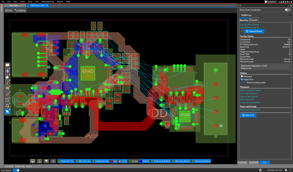
Once the board is laid out, it must be proofed or verified, as well. The most significant testing is for DFM, DFA, and other constraint compliance. This is known as design rule checking (DRC) and virtually all design tools include a checker that performs this vital evaluation. Another useful verification is layout versus schematic (LVS) testing, which compares a netlist generated from the board layout with the schematic netlist.
Other tests and simulations are also essential during this step to avoid building boards that fail to meet performance standards and/or adhere to industry compliance standards–such as USB, MIPI, PCIe, and others. Common simulations are signal analysis, power delivery network; also known as power distribution network (PDN) testing, and thermal distribution evaluations. The latter two are powerful analyses that help you choose heat dissipation devices and techniques.
The Importance of Layout Efficiency
For all but the simplest of designs, producing electronic circuit boards is a complex endeavor that involves many professionals and multiple companies. Typically, there is a primary board designer, a reviewer (usually a more experienced engineer that specializes in an area; such as RF analysis), an MCAD engineer to design an enclosure or integrate mechanical functionality, a testing engineer to verify performance and operation, and the fabrication and assembly house teams, often including engineers and technicians. Everyone involved relies upon the quality and efficiency of the PCB design process, which includes the following stages:
PCB Design Process Stages
- Selecting the Components
The first stage of the PCB design process is arguably also the most important. Your choice of components directly affects the board layout, manufacturing, circuit performance, and reliability. With the many choices of parts available and the supply chain challenges such as delays, obsolescence, and counterfeits, it is imperative that you follow best practices for sourcing and proofing the component models and employ effective component library management.
- Drawing the Schematic
The complexity of the schematic is directly proportional to that of your design. Often, a good schematic can consist of a single well-organized page that includes the circuit drawing, references, and pertinent information, like the title block that identifies when the schematic was created and reviewed and by whom. More common; however, your schematic will consist of multiple drawings and pages. In either case, it is important that standardized symbols — for example, ANSI Y32.2 Graphic Symbols for Electrical and Electronics Diagrams — are used to maximize readability as you step through the major stages of schematic generation.
- PCB Layout Design Process
The PCB layout is the culmination of the designer’s interpretation of the performance objectives and design intent integrated with engineering best practices, which must adhere to industry standards and physical constraints. The complexity of this process often means it is the most difficult to perform efficiently.
- Preparing for Manufacturing
The last stage of PCB design processing is to compile all data, information, and imagery that is needed by your CM to build your board. It must reflect your design intent, and meet your performance objectives. These are encapsulated in the bill of materials (BOM), which provides data and information about the components selected, and the design file(s) that include the schematic drawing, netlist, drilling requirements, board layout, and all other important text and imagery to be used for the board build.
Each of these stages is essential and builds upon the results of the previous stage, as is explained above. However, the PCB layout design process is most often the most challenging and time-consuming. Consequently, employing an advanced PCB layout software tool, such as OrCAD X Presto, is key to optimizing efficiency. Partnering with the industry leader for meeting engineers’ PCB design software and support needs is the best option for achieving your PCB layout design process goals.