This class will cover a detailed review of all the necessary steps for designing a printed circuit board, from loading logic/netlist data through producing manufacturing/NC output. Attendees will receive in-depth training on placement, constraint management, shape creation and editing, as well as important tips from our PCB design experts to ensure you are able to get the most out of OrCAD PCB Editor.
This class is a comprehensive course aimed at helping students learn an efficient, front-to-back schematic and PCB workflow. This package includes Capture Essentials and PCB Editor Essentials training.
Take your OrCAD PCB Editor skills to the next level with our advanced class. This class will provide in-depth training in advanced topics such as constraint management, auto-interactive routing, differential pairs, as well as time features such as design reuse and tech files. Become more efficient and get your products to market faster with this class.
It is recommended that students have a pre-requisite knowledge and proficiency in OrCAD Capture Schematic editing and PCB Editor.
Customizing the OrCAD and Allegro PCB Editor Environment
PSpice® Essentials for Simulation training builds on the design entry essentials learned in the Capture class and adds new skills to enable simulation directly from the Capture environment. This class is ideal for both new PSpice® users and experienced engineers who need to maximize the performance of their circuits. Students should have recently completed the one-day Capture Essentials class as this class builds on the schematic design foundational skills learned in that class
Includes an OrCAD Certification Opportunity.
There are no prerequisites for this course.
Run DC bias, DC sweep, AC sweep, and transient analysis
Edit stimulus to create any kind of input waveform
How tolerances work and how they affect convergence
Run sweeps using parametric analysis
Bring models from the internet into PSpice
Run monte carlo and worst case analysis’
Create linear and non-linear transformers
Model parts mathematically using ABMs (Analog Behaviour Models)
This class is a comprehensive course aimed at helping students learn an efficient, front-to-back schematic and simulation workflow. This package includes Capture Essentials and PSpice Essentials training.
Includes an OrCAD Certification Opportunity.
There are no prerequisites for this course.
How to build new parts and symbols
Design-checking best practices
Techniques for assigning reference designators
Creating a BOM (Bill of Materials)
Adding part and net properties
Creating flat designs
Run DC bias, DC sweep, AC sweep, and Transient analysis
Edit Stimulus to create any kind of input waveform
How tolerances work and how they affect convergence
Run sweeps using parametric analysis
Bring models from the internet into PSpice
Run Monte Carlo and Worst Case analysis’
Create linear and non-linear transformers
Model parts mathematically using ABM’s (Analog Behavioral Models)
Learn how to optimize your design for cost, yield, and manufacturability with our PSpice Advanced Analysis class. This class is ideal for those who need to automatically maximize their circuit performance using PSpice Advanced Analysis.
It is recommended that students have a pre-requisite knowledge and proficiency in OrCAD Capture Schematic editing and PSpice.
Your Trusted Source for Complete PCB System Design & Analysis Software
EMA Design Automation is your full-service provider of CAD software, services, 5-star support, and content you need to drive innovation in your products.
From design, through analysis, verification, and release to manufacturing we have the best-in-class design solutions to help solve your toughest challenges reliably and repeatably.
Explore our comprehensive end-to-end electronic system design solutions built to scale and grow with you.
PCB Design
Access the only unified, scalable PCB design platform built to grow with you. Design, analyze, manage, and build all within a single environment with best-in-class in every class technology.
Managing your design & libraries should not require a whole new set of tools and personnel. Explore our integrated design and library management solutions to enable fast, efficient, and traceable data & library management all built inside the CAD tools you use every day.
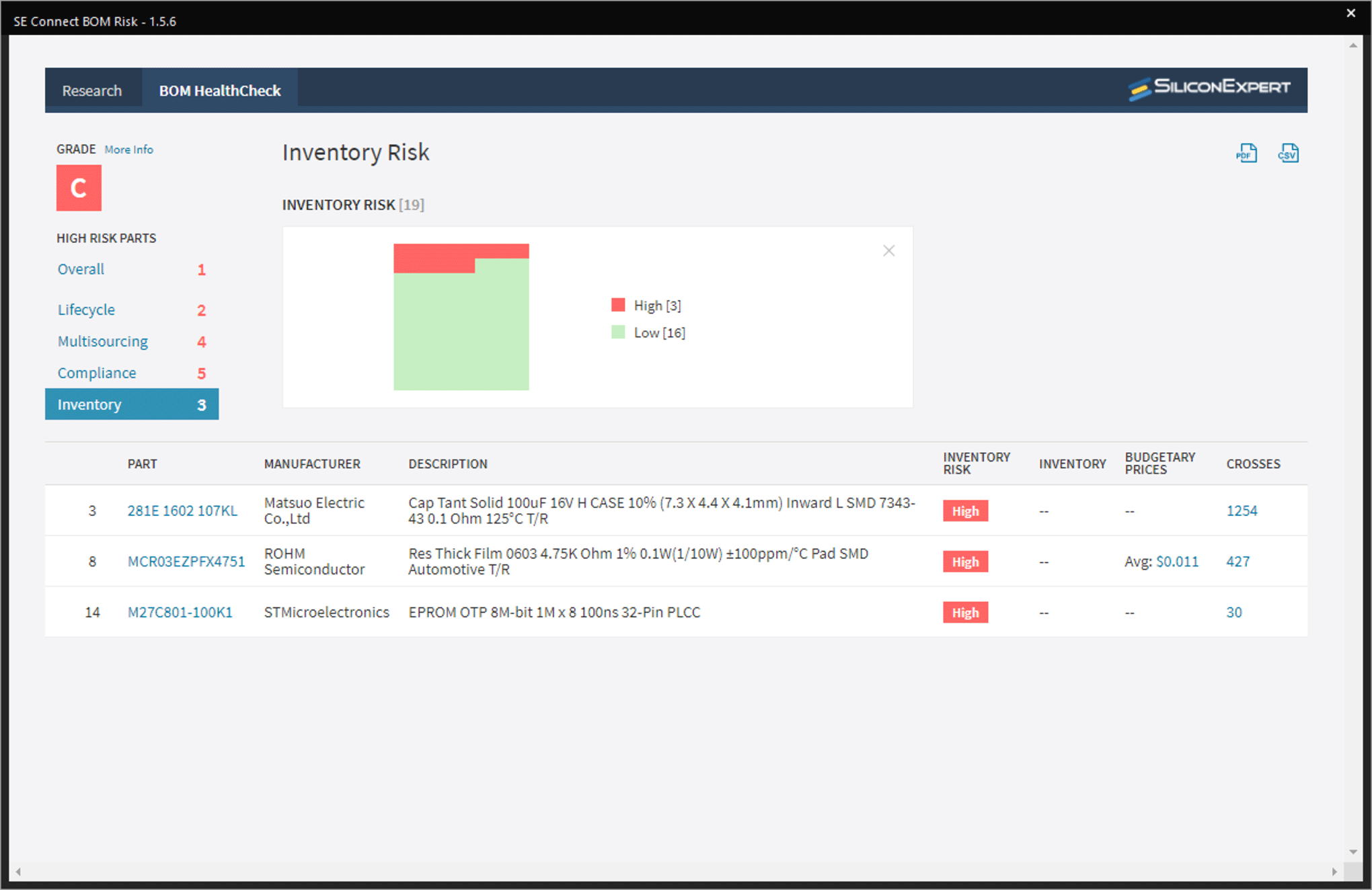
Identify and prevent part availability, obsolescence, lifecycle, and more while designing with embedded real-time supply chain data. Solve supply chain problems before they happen to ensure a smooth path to production.
Solve todays multi-faceted, multi-domain electrical design challenges with a complete portfolio of analysis solutions. From SPICE, to Signal & Power Integrity, RF, Microwave, EMI/EMC, and Thermal, quickly and accurately create complete virtual prototypes of your designs for reliable first pass success.
Electrical and mechanical design requirements are more intertwined than ever. See how EMA enables seamless collaboration between ECAD and MCAD with automated change tracking, change approvals, and native file support.
More than Moore means looking at new ways to continue pushing the design envelope. Packaging advancements provide a powerful way to drive performance, cost, size improvements in your designs. Explore our industry leading solutions for 3d-IC, CoWOS, INFO, and more.
Where the ruber meets the road and your idea becomes a reality. Our integrated DFM and product release solutions allow you to prepare and check for manufacturing from the start and send your products to be built with confidence.
Our Services
For over 30 years EMA has been proudly serving the EDA community
EDA CAD Software
Complete range of software to help you design, analyze, verify, build, and maintain your electronic products.
New Digi-Key OrCAD Bundle Addresses Component Lead Time
and Availability Challenges by Providing Engineers
with In-Design Access to Critical Component Data and Libraries
Rochester, NY (August 17, 2021) – EMA Design Automation® (www.ema-eda.com), a full-service provider and innovator of Electronic Design Automation (EDA) solutions and Digi-Key Electronics, which offers the world’s largest selection of in-stock and ready-to-ship electronic components, have collaborated to release the OrCAD® Capture Bundle, a special offer available only on digikey.com.
This new design bundle provides the tools, data, and models needed to ensure first pass design success including:
-OrCAD Capture, the industry-standard schematic design solution -In-design ability to search and select parts from Digi-Key -Searchable cloud library of schematic symbols connected to Digi-Key parametric data -Integrated sourcing tools to procure parts quickly and easily from Digi-Key -OrCAD e-Learning, including certification opportunities
This unique collaboration furthers both EMA’s and Digi-Key’s goal of increasing the efficiency of engineers by providing the tools they need to streamline the design process. Now, engineers can focus on design, eliminate tedious tasks, quickly innovate, and keep the design process moving forward, all within a single unified design environment.
“We have always been focused on improving the engineer’s workflow and providing them access to the data they need as they are making important design decisions,” said Manny Marcano, President and CEO of EMA. “This announcement is an extension of our longstanding collaboration with Digi-key to enable engineers with best-in-class design methodologies and data.”
With the current uncertainty in the global electronics supply chain, it is more critical than ever that engineers have access to the information they need to make informed part decisions. By connecting the vast Digi-Key database of part parametric information with the industry standard in PCB schematic design, engineers now have an integrated “supply chain ready” path to confidently create manufacturable designs quickly and accurately.
“Part availability and lead time are a huge concern for companies around the world,” said Travis Foss, Product Manager, Semiconductors, at Digi-Key Electronics. “Enabling engineers to have a view into this data right at product conception gives design teams the foresight they need to make the right choices and go to production with confidence. Digi-Key is thrilled to be able to offer this unique solution.”
The Digi-Key OrCAD Capture Bundle is available for purchase now worldwide. To learn more visit https://go.ema-eda.com/dk-orcad-capture-bundle.
About EMA Design Automation
EMA Design Automation is a trailblazer in product development solutions offering a complete range of EDA tools, PLM integrations, services, training, and technical support. EMA is a global Cadence Channel® Partner, serving all of North America, United Kingdom, Ireland, India, and South America. EMA develops Ultra Librarian®, TimingDesigner®, CircuitSpace®, CIP™, EDABuilder®, and a host of custom solutions to enhance the OrCAD® and Dassault products, and all are distributed through a worldwide network of value-added resellers. EMA is a privately held corporation headquartered in Rochester, New York. Visit EMA at www.ema-eda.com for more information.
About Digi-Key
Digi-Key Electronics, headquartered in Thief River Falls, Minn., USA, is recognized as both the leader and continuous innovator in the high service distribution of electronic components and automation products worldwide. As the original pioneer in this space, Digi-Key provides more than 11.7 million components from over 1,900 quality name-brand manufacturers with an industry-leading breadth and depth of product in stock and available for immediate shipment. Beyond the products that drive technology innovation, Digi-Key also supports design engineers and procurement professionals with a wealth of digital solutions and tools to make their jobs more efficient. Additional information can be found at digikey.com and on Facebook, Twitter, YouTube, Instagram and LinkedIn.
# # #
EMA Design Automation, TimingDesigner, CircuitSpace, EDABuilder, Ultra Librarian and the EMA logo are registered trademarks, and Component Information Portal is a trademark of EMA Design Automation, Inc. Cadence, Allegro, and OrCAD are registered trademarks of Cadence Design Systems, Inc. All other trademarks in this release are the property of their respective owners.
“Designing a product is designing a relationship,” says industrial designer, Steve Rogers. It’s true, consumers do relate best to products that solve their problems. Take for instance the following scenario:
Problem: I cannot manage to catch my favorite TV show when it airs on TV as I am asleep.
Solution: The birth of the VCR (Video Cassette Recorder).
Every product to come to market has undergone some form of the design process. The product design process typically begins with concept ideation and ends with the finished product. In between these two points there are certain design process phases, each with its own rules and sub-processes. By understanding the overall product design process, you will be empowered to engineer innovation into the finished product that will make consumers relate to it in powerful ways.
By looking at a case study simulation informed by both real-world experience and industry best practices, we’ll uncover how freelance engineers might best use the product design process to create fantastic products that not only fulfill the client’s brief, but also solve the consumer’s problem.
Imagine a client requests very specific outcomes, but makes no hardware specification or other information. In this instance, the role of the freelance engineer is to understand the problem from a layperson’s perspective. The details can come later. Next, we’ll show how the use of non-technical language helps better define the exact nature of the problem being addressed and thus begins the product design process in earnest.
Initiating the product design process: Inception
Client: I would like to make a device small enough to fit into the palm of your hand but also powerful enough to detect different things in its immediate environment. I need this product to be able to tell how far it is from other objects and then move or stop some motors as needed. Or, do something like play a noise if someone walks past it. It would be great if it could also drive a mini car around by wireless joystick.
You: Ok, so you need something that can make decisions in real time based on information it is receiving from its sensors?
Client: Correct. And I want it cheap enough that most people can afford to buy it, but it still makes me a decent profit because it uses cheaper parts.
You: Alright, let me get this right. You don’t want this product to have a bunch of expensive chips or parts. You only want a design with a chip that is smart enough to interact with various types of sensors.
Client: Yes. I want everyone from a technology expert to an absolute beginner to be able to use this product in creative and fun ways. Users should be able to add or subtract sensors depending on how their application. Making it easy to use is important as we want people to have fun with the product. This will help it sell well.
You: Makes sense. How soon are you wanting the first prototype?
Client: Well since it shouldn’t be too complicated, how about 2 months?
You: Yeah, I can do that.
Simple. Straightforward. Succinct. Notice how important it is to understand the needs and wants of your client as well as the nature of the problem the product is being designed to solve? This why using non-technical language is beneficial. It allows for clear communication between client and designer and lets the focus be on the bigger problem and not the technical minutiae.
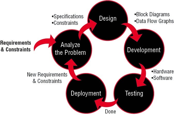
The product design process explained
Now that you have clearly defined the problem as well as the client’s requirements, it’s time to start designing. The following diagram helps explain how the different phases with the product design process are interconnected and inform each other.
As you can see, the product design process moves through multiple phases but begins with a singular dynamic: the needs of the client. Remember, it’s important to clearly understand the problem before moving onto the latter stages of the design process. If we fail to fully comprehend our client’s requirements and constraints initially, we run the massive risk of producing a product not fit for purpose. This means, as a freelance engineer, you don’t get paid! With this in mind, let’s investigate each step of the product design process in more detail to see how we can engineer fantastic products that solve problems.
Phase 1 – Analyzing the Problem
Requirements and constraints are not only two different things, sometimes they work in opposition. Obviously, requirements are the features we want a product to have, whereas constraints are the mechanical and electrical limiting characteristics of the product. No matter what, it is essential to nail down the requirements and constraints of the product you are designing first and foremost.
Looking back at the simulated conversation at the beginning of the article, the requirements for the product are as follows:
USB-powered and USB-programmable
Able to be reset
Handle ICSP, I2C, and SPI communication protocols
Analog to Digital conversion to deal with external interaction
Output pulse width modulation (PWM) signals
And the constraints for the product are:
Handle a decent input voltage range (around 6 to 20 V max)
Be about the size of a deck of cards
Operate at 5 V
Needs to be ‘light’
Now your role as an engineer is to translate these high-level concepts into electrical and mechanical specifications and constraints. To systematize this process, do the following:
Write down the desired outcomes (e.g. fall detection)
Break down the desired outcome goals into fundamental physical phenomena (e.g. jerk and acceleration detection)
Research devices that perform the specific measurement or action described by the physical phenomena (e.g. an accelerometer)
Write down the requirements for how quickly, accurately, and efficiently the device needs to meet the desired phenomena (response time, voltage, current, power ratings, bandwidth, etc.)
Voila! Now you have a way of working out the specifications and constraints for the project. In dot-point form, these might look like:
Specifications:
A specific kind of microcontroller that handles all the types of communication requirements
A USB controller chip to handle USB flashing and communication
Operating voltage – 5 V
Input Voltage – 7-12 V
Digital I/O Pins – 14
Clock Speed – 16 MHz
Constraints:
Length – around 2.8 inches (~71 mm)
Width – around 2.2 inches (~56 millimeters)
Weight – 30 grams
Phase 2 – Design
Now that you have your requirements and constraints, you and your partner can define the mechanical (e.g. enclosure) and functional (e.g. block diagram) parts of the product. Let’s look at one way of conceptualizing this.
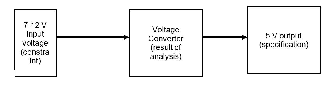
Block Diagrams / Data Flow Diagrams
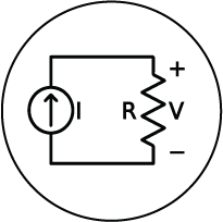
I am a strong advocate for visualizing the concepts of any design. The best way to do this is to use a simple block diagram to show how the requirements of the project can be achieved. For example, one requirement might be to "take in 7 V and output 5 V". To meet this requirement, the block diagram looks like this:
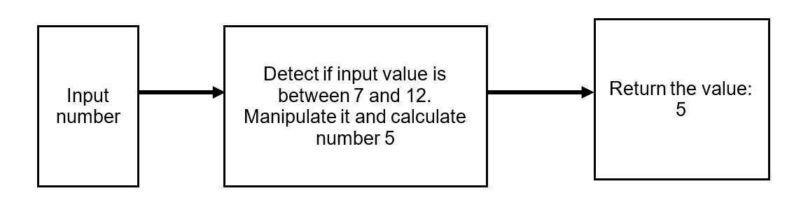
The next part of the product design process is to think in terms of software programming. The voltage converter block would be a function. This function/block takes an input and gives a desired output. For example, you can write code that takes any value between 7 and 12 and always outputs the number 5. In that way, the voltage converter is the same as the code that converts 7-12 to 5.
Whether you’re working with software or hardware, it’s important to use function blocks throughout the entirety of your project until you turn all project requirements into outputs. Now you are ready to develop devices or code to actualize those function blocks.
Phase 3 – Development
Knowing exactly the kinds of devices or code functions you need to meet your function requirements is critical to the product design process. Now, within the Development phase of the process, it is time to develop your function block map. This involves:
Designing devices that perform the task of each function block
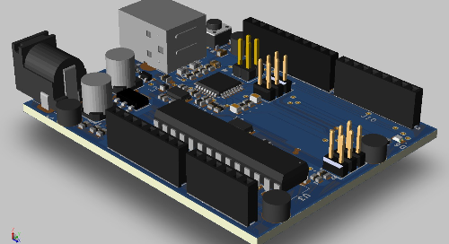
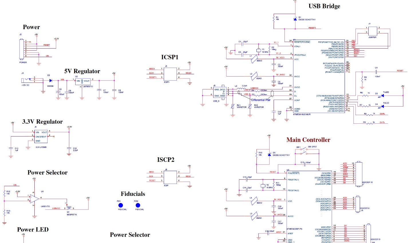
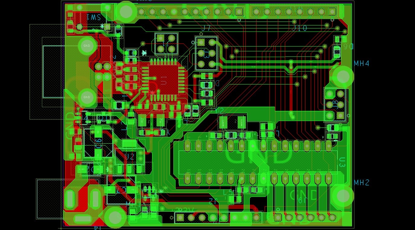
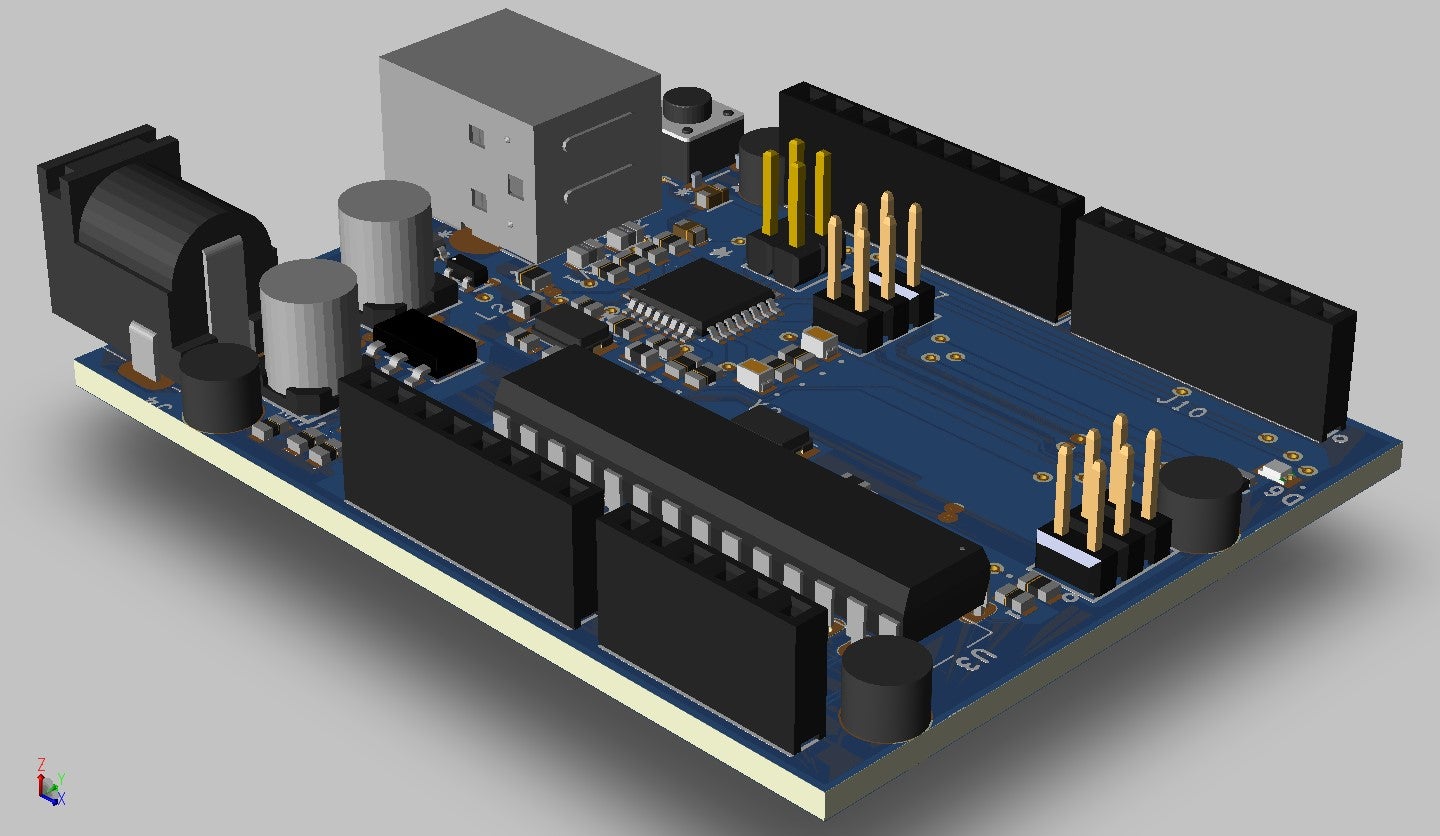
Creating high-level concepts/blocks which connect the devices and code so they can work together (for electronics this is what is known as a schematic)
Checking parts/code work individually whilst building the main schematic
Checking parts/code still work after connecting them and the schematic has been built
Full schematic of multi-sensor PCB
Now you are ready to move on to the next phase of the product design process: testing the developed schematic through a design review.
Phase 4 – Testing and Documentation
So far, the first three phases in product development (analysis, design, and development) have allowed us to create a conceptual solution which meets the client’s product requirements. But how can we be sure the actual product we are designing will work? The surefire way is to test it.
Pro tip: Never skip the testing phase.
So how do you go about testing a developed design? In a nutshell, there are two main ways: review-based testing and simulation testing. Review-based testing means checking your schematic’s components function correctly to see if the intent behind your product design is functionally sound. Simulation testing goes a level deeper to evaluate a circuit’s behavior in real time, whether by calculator or software.
Review-based (Logical) Testing
Once you have verified, to a high level, the product design is sound (i.e. function blocks are where they should be, voltage modifications are performed by certain parts of a circuit, and so on), it is time to look at reviewing the following key factors:
Current supply for devices: Do your power supplies provide enough current to power your all devices?
Voltage levels across devices: Is there a voltage mismatch among your parts that would cause them to not operate?
Pin connections: Are the right pins connected to each other (e.g., input signals to output signals)?
Missing or unnecessary devices: Once you have determined all connections, pins, wires, voltages, and current ratings for devices are correct, check for any unnecessary parts in your design and remove them. Or if there is something missing, then add it. Following the steps in this list will help to reveal missing devices that should have been included within earlier stages of the product design process.
Now that we have verified the correct devices are connected to the correct wires and symbols, we are ready to see how the circuit behaves when power runs through it. This is known as functional or behavioral testing (or simulation).
Functional/Behavioral Testing
After checking the parts, connections, and deciding the design is a valid one, it’s important to simulate the product’s behavior wherever possible as it will help reveal errors a design review won’t.
Please note: There are two different ways of conducting a ‘simulation’. One way is via a physical simulation (hardware testing) and the other, more common way, is running a software simulation. We will focus on software simulation of the design.
Simulation
Simulation testing prevents the problem of finding out your product does not work after you already built it. Therefore, this type of testing is indispensable to the product design process as it can save you a lot of time and money.
From previous experience, I could have avoided losing $30,000 in testing and transportation costs and another $20,000 in man-hours, if my team and I had just spent $4000 to run a simulation software test on our project.
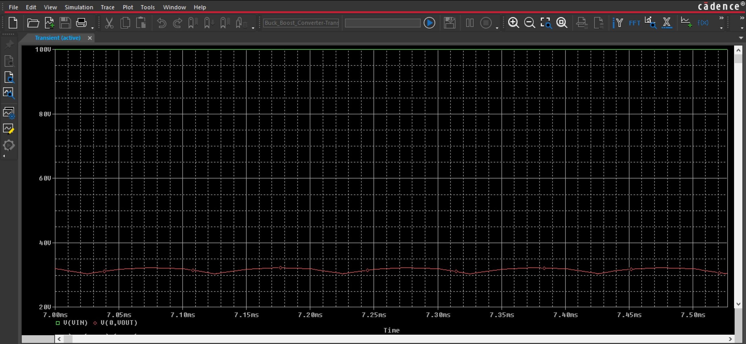
Using circuit simulation tools like OrCAD PSpice will show how your circuit schematic behaves in real-time. With analog designs, this feature is worth its weight in gold. And, at this phase of the product design process, you are doing your own functional testing.
There is no substitute for testing a hardware product in the real world with your own hands. However, simulations can go a long way in detecting problems early and therefore, make the problem easier to fix earlier in the process.
As you conduct product testing it’s important to record all the relevant results. This will help you maintain excellent documentation, a crucial step in the overall product design process, which we will now look at in more depth.
Feedback and Documentation
Proper documentation is invaluable. Not only can it save unbelievable amounts of time, it also makes it easier when your product undergoes review. Imagine you get asked to review a project that had little to no documentation. You would not know how to begin and would most likely find it very difficult to figure out what steps were taken in designing the product.
Pro tip: Keep all notes, thoughts, ideas, additional documents, and anything else you might need in one central location or document that is easy for the rest of the team to access. This provides stakeholders who have questions about a design/product the ability to refer to the documentation without having to rely on you to supply them with answers.
Engineers might stay in the phases of design, testing, and documentation for a long time. While the process in these phases can be quite tedious at times, it is always worth it in the end. Adhering to this process will grant your product the best chance of working properly and solving your client’s requirements.
Phase 5 – Deployment
Within this phase we are essentially making it easy for the receivers of the product to understand exactly what you made and how to use it. Indeed, having others immediately understand your product is the height of engineering sophistication and positive user experience.
To achieve this, you need to have documentation such as:
Circuit board fabrication data
Product user guides
Quick start guides
Data sheets
Drawings of the design
Example code, etc.
You may also need extra documentation such as patent protections, bill of materials, etc. to gain certification for your product(s). As you can see, a lot more goes into deployment than one may initially think.
External Feedback
After deployment, now it is time to receive feedback about our product from either the client, outside organizations, the public, or all three. Maybe a decision is made to have the product interact with more sensors, or maybe it needs to be powered by a different type of charging peripheral. This type of feedback is valuable as it helps us form new design requirements and constraints for future versions of the product.
Conclusion
Good product design requires knowledge, imagination, and creativity.
The product design cycle is a practical way to ensure you create a great product people will truly appreciate because it solves a problem. Whenever you get a new idea, problem to solve, or entire project to work on, it is important to do the following:
Analyze the problems and sub-problems to create specifications and constraints
Visualize the high-level concept of the product to meet the design needs and specifications (block diagram)
Find or create the parts and software that go into the block diagram and are needed to make everything work together (schematic)
Virtually test (simulate) what you developed to see if it works before buying hardware
Document and share your work
Once your work is shared, be open to feedback to improve your product and in turn, your skills as an engineer. Self-improvement as an engineer keeps you competitive and gives you better options in the future, as does the reputation of producing quality designs. While transforming a client’s ideas and requests into a fully functional product may seem complex and over-whelming at first, having a tried-and-tested design process as your basis means you can deliver a highly successful product every time. Establishing a solid design process will allow you to consistently deliver excellent products on time.
EMA OrCAD e-Learning teaches OrCAD design tools at your own pace with self-guided, online training classes. Includes one-year access to videos, labs, and comprehensive training materials for OrCAD® Capture, CIS/CIP, Engineering Data Management, PCB Editor, and PSpice courses.
Course Overview: Learn all the necessary steps required to create a schematic using OrCAD Capture. New users will learn the essentials needed to generate a design, how to navigate the tool, run DRC checks, prep the design for netlisting, and generate BOMs. Prerequisites: There are no prerequisites for this course. What You Will Learn:
Course Overview:PSpice® Essentials for Simulation training builds on the design entry essentials learned in the Capture class and adds new skills to enable simulation directly from the Capture environment. This class is ideal for both new PSpice® users and experienced engineers who need to maximize the performance of their circuits. Students should have recently completed the one-day Capture Essentials class as this class builds on the schematic design foundational skills learned in that class Prerequisites: There are no prerequisites for this course. What You Will Learn:
Run DC bias, DC sweep, AC sweep, and transient analysis
Edit stimulus to create any kind of input waveform
How tolerances work and how they affect convergence
Run sweeps using parametric analysis
Bring models from the internet into PSpice
Run monte carlo and worst case analysis’
Create linear and non-linear transformers
Model parts mathematically using ABMs (Analog Behaviour Models)
Course Overview: This one-day class will cover component data management with Cadence OrCAD Capture CIS and the OrCAD Component Information Portal™ (CIP), including product interface fundamentals, automating the part introduction process, and effectively managing the part database. Prerequisites: It is recommended that students have a pre-requisite knowledge and proficiency in OrCAD Capture Schematic editing. What You Will Learn:
Manage parts and symbols in a relational database
Assign user privileges
Track historical changes of active and legacy parts
Manage the integrity of active and historical parts
Use distributor searching to locate necessary parts
Align new part introduction with corporate protocols
Course Overview:OrCAD EDM (Engineering Data Management) is a collaborative environment which enables teams of engineers to work on a single Cadence OrCAD Capture design file. This course will provide you with the necessary knowledge required to effectively manage your team within the OrCAD EDM Environment. New users will learn how to navigate the tool as well as tips and tricks on how to get the most out of the product. This course takes approximately 5-6 hours and is available as a one-day Virtual Training. Prerequisites: It is recommended that students have a pre-requisite knowledge and proficiency in OrCAD Capture Schematic editing. What You Will Learn:
How to assign roles based on tasks
How to set up users, assign privileges
Template and project best practices
How to manage libraries and assign symbols to team members
Adding parts to master libraries
How to activate OrCAD EDM within PCB Editor so all PCB and related files become a part of EDM-managed projects
We here at EMA are committed to your success. Our e-learning course is perfect for those that want to learn at their own pace. Don’t see an option that meets your needs? We can tailor a course to meet your unique training requirements.
E-LEARNING
Learn at your own pace with our self-guided, online training classes complete with videos, labs, and comprehensive training materials.
Don’t see an option that meets your needs? We can tailor a training class to meet your unique requirements.
“Hats off to my instructor, Mr. Harms, his enthusiasm, knowledge, & presentation were the very best I have experienced in the many training classes I have attended!”
Users who register for select classes gain access to our OrCAD certification test. Certifications are designed to help students demonstrate their mastery of OrCAD products.
A detailed review of all necessary steps for designing a printed circuit board, from loading logic/netlist data through producing manufacturing/NC output.
When you decide to purchase an OrCAD product, we want to do everything in our power to ensure your success. Our goal is for you gain the knowledge and skills needed to help you get up and running quickly and ensure you maximize the return on your OrCAD purchase.
To achieve this, EMA offers a variety of difference types of training sessions – from classroom training to e-learning—each tailored to different learning styles.
Learn in a way that works for you
What sets EMA apart is our immense selection of training options. It allows you choose the format best suited to your learning style and company goals. Course types offered include:
Classroom training
Hands-on, in-person training courses. Regional classes are offered several times a year in locations close to you.
Virtual training
Virtual training classes feature a live instructor who will teach your team over the internet.
E-learning
Learn at your own pace with our self-guided E-learning online training classes. Our e-learning classes come complete with videos, labs, and comprehensive training materials—all you need is a computer and an internet connection.
On-site training
Our training staff will come to your location and provide training so you don’t have to leave your office.
Custom training
OrCAD training classes tailored to your unique requirements and timeframe.
Our Classes
We aim to provide training that is relevant, timely, convenient, and cost-effective. Each class offered covers a specific software, aimed at helping attendees accomplish specific tasks. Classes offered includes:
OrCAD Capture
OrCAD Capture CIS
Component Data Management
Intro to PSpice
Simulation with PSpice
PSpice Advanced Analysis
Intro to PCB Editor
OrCAD PCB Editor
Advanced PCB Editor
Our Instructors
Our courses are instructor-led (with the exception of e-learning) and taught by some of the industry’s best instructors who are proven experts in their field, OrCAD certified. Our instructors are highly knowledgeable professionals with typically 20 or more years of real-world experience. Their expertise will help to ensure you will find success with whatever course you enroll in.
Your experience is important to us, and in order to ensure you high-quality training, we administer class satisfaction evaluations at the end of each course. This helps us to ensure students are happy with the instructor’s performance. Based on our evaluations, we have found that 9 out of 10 students confirmed the class they attended exceeded their expectations.
OrCAD Certification
We are excited to announce we have recently launched a certification program for our Capture, PCB Editor, and PSpice software. Our certifications are designed to validate and recognize the technology specializations and skills PCB designers and indicate they have the knowledge required to successfully utilize OrCAD products.
Upon completion of our certification process, the trainee receives an official OrCAD certification, as well as an official OrCAD certification image badge they can display on the company website, social media, etc.—validating their ability to plan, design, and implement our software.
Invest in Yourself
Whether you’re just starting implementation, have undergone staff changes, or are looking to update your skills, EMA’s training programs provide you with the expertise to help you use OrCAD solutions to their fullest potential. No matter how complex your environment is or where you are located, we are sure to have a training solution for you.
Visit our Learning Overview to learn more about our training classes.
Recently, Arrow teamed up with Cadence to provide integrated design tools to engineers, creating an accelerated path for new product development and the ability to bring products to market faster and cheaper.
Now, thanks to this collaboration, customers will have access to qualified components while using Cadence’s PCB suite, enabling them to deliver innovative designs to market swiftly. For Arrow, having the OrCAD suite of design tools in their portfolio now allows them to better support engineers by enabling them to create and deliver reference designs in OrCAD formats to users who already utilize OrCAD design tools.
In addition to Arrow’s collaboration with Cadence, Arrow has also partnered with INDIEGOGO, a website where startups and entrepreneurs can receive funding from the public for their products. With the formation of these powerhouse partnerships, we decided to feature startups and small tech companies within INDIEGOGO on our blog each month.
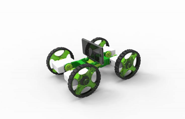
We couldn’t think of a better company to kick this series off other than Ziro, the world’s first hand-controlled robotics kit. Ziro offers several kit options: out of the box, pre-made toy kits, or make your own.
A recipient of the Best of CES Finalist in 2016 award, this robotics kit also allows you to design and build your very own creations. With easy control and endless possibilities, this is a great item for beginners, as well as those who want to bring a creative twist to robotics.
What sets this robotics kit apart from the rest is the Arrow Certification. This certification helps establish the trust backers need to provide the upmost support for a product. With this support and certified review by a team of engineers, there’s no wonder why companies such as Ziro are successful. During the certification process Arrow’s own engineers provide feedback and analyses regarding bill of materials optimization and design-for-manufacturing review, ensuring the product is ready for production and beyond with no foreseeable setbacks.
Ziro has wrapped up their campaign, and is currently in manufacturing and assembly process. Want to purchase your Ziro kit today? Visit Indiegogo’s website or the Ziro website here today to learn more.