How to Use LiveBOM

With supply chain shortages and part delays becoming the new normal, assessing component availability and lifecycle status during the schematic design to ensure the parts chosen will be available when the design is ready to produce is critical. LiveBOM, included in OrCAD X, is a new tool that takes these worries away by tracking the status of each component and providing real-time supply chain data in your design.

This quick how-to will provide step-by-step instructions on how to use LiveBOM in OrCAD X Professional.

To follow along, download the provided materials above the table of contents.

How-To Video

Open in New Window

Activating LiveBOM

Step 1: Open the provided design in OrCAD X Capture CIS.

Note: Make sure to open OrCAD X Capture CIS with a license of OrCAD X Professional. Log in with your Cadence username and password if prompted.

Adding a Design to Workspaces in OrCAD X Capture CIS

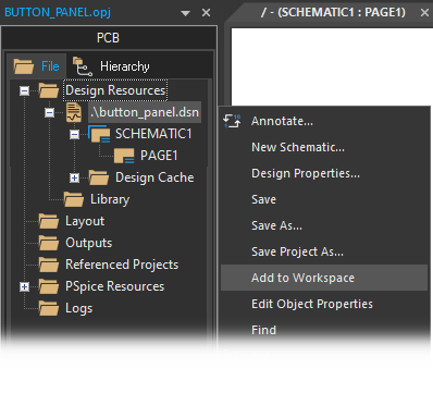
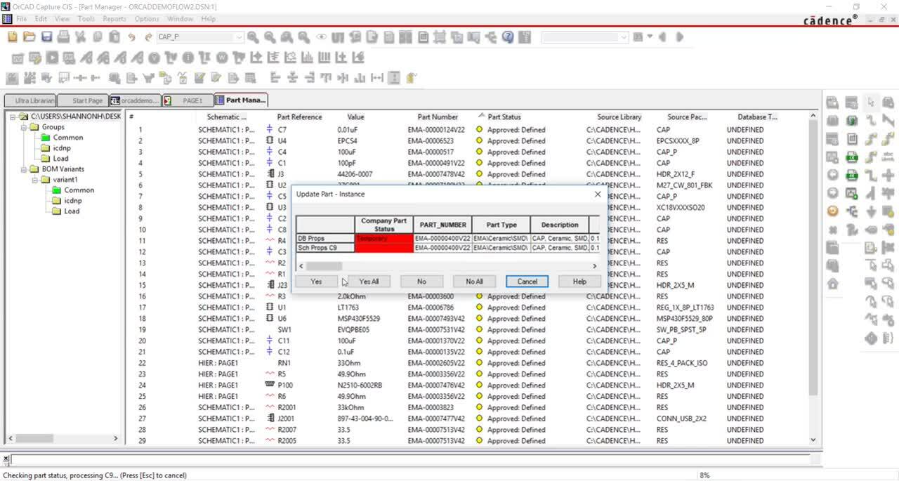
Step 2: Right-click the DSN file in the Project Manager and select Add to Workspace. This will add your design to your workspace to access LiveBOM.

Step 3: Select Tools > Live BOM from the menu.

Note: If you receive a prompt that the LiveBOM data must be regenerated, click OK, save the design file, then select Tools > Live BOM from the menu again.

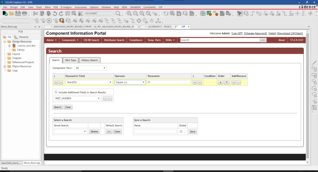
Navigating the LiveBOM Interface

Use LiveBOM to analyze at-risk components with real-time supply chain information.
LiveBOM in OrCAD X

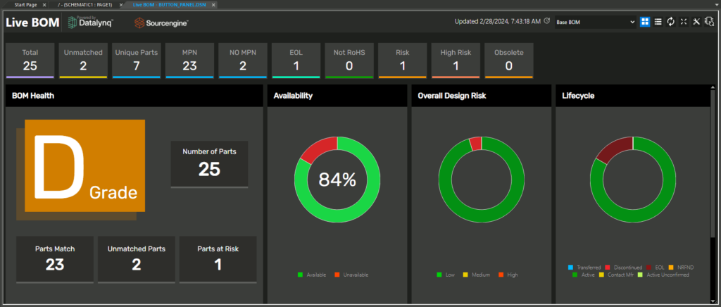
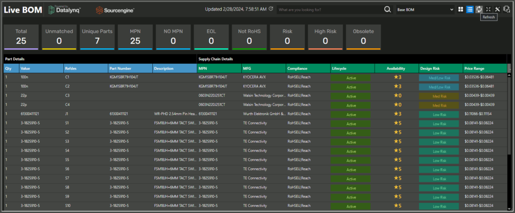
Step 4: View the LiveBOM interface. At the top of the window, there are several categories for parts including:

  • Total: The complete list of parts.
  • Unmatched: Lists all parts with no matching manufacturer part number (MPN).
  • Unique Parts: Lists all unique part numbers used in the design.
  • MPN: Lists all parts with a manufacturer part number.
  • No MPN: Lists parts with no matching MPN.
  • EOL: Lists parts at the end of their active life.
  • Not RoHS: Lists parts that are not RoHS-compliant.
  • Risk: Lists parts that are considered at risk.
  • High Risk: Lists parts that are considered at high risk.
  • Obsolete: Lists parts marked as obsolete.

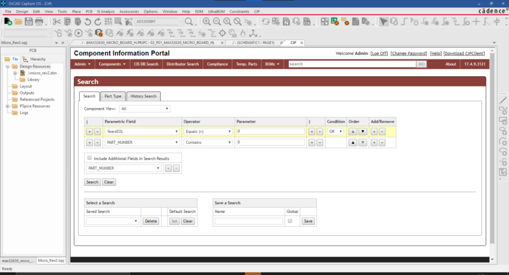
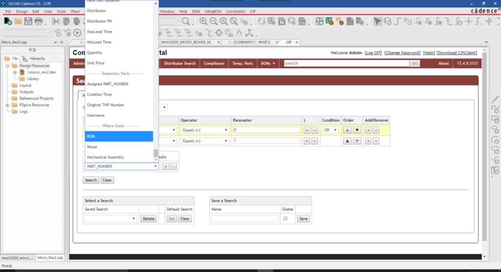
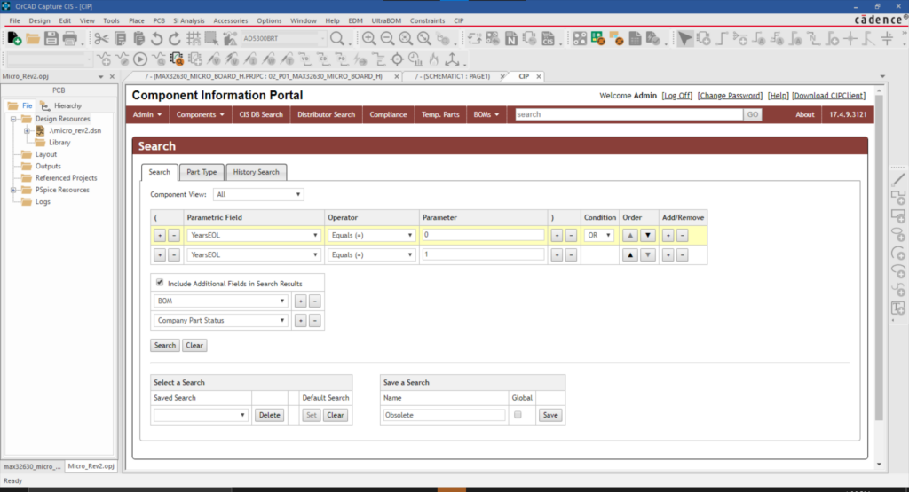
Selecting a category will turn its filter on or off.

The BOM Health Panel in LiveBOM

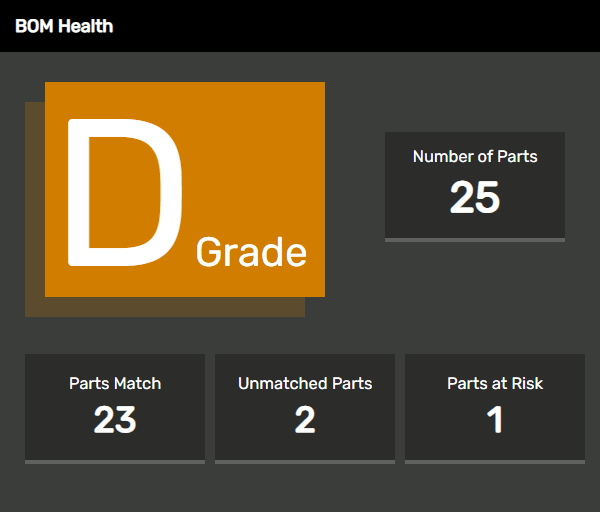
Step 5: View the BOM Health panel. This panel shows a letter grade for the design based on the number of parts matched, their availability and their risk. The numbers of matched, unmatched, and at-risk parts are also shown. Currently, the design has a grade of D, as two parts are unmatched and one is at risk.

Risk Charts in LiveBOM

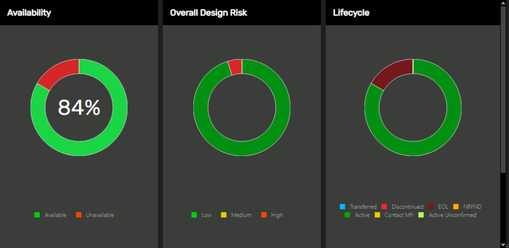
Step 6: View the pie charts on the right side of the window for Availability, Overall Design Risk, and Lifecycle. The charts are mostly green, indicating low risk.

Risk Tables in LiveBOM

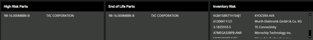
Step 7: Scroll down to view the tables for High-Risk Parts, End of Life Parts, and Inventory Risk parts. The part with manufacturer part number 9B-16.000MBBK-B is listed as a high-risk part and end-of-life part, as it is considered obsolete.

Use LiveBOM to Replace High-Risk Parts

Note: All at-risk parts can be viewed in the Risk Category.

Step 8: Select Risk from the top to view the list of at-risk parts.

Viewing Part Properties

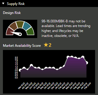
Step 9: Select the row for Y1. Under Supply Risk in the Properties panel, the part is listed as “may not be available.”

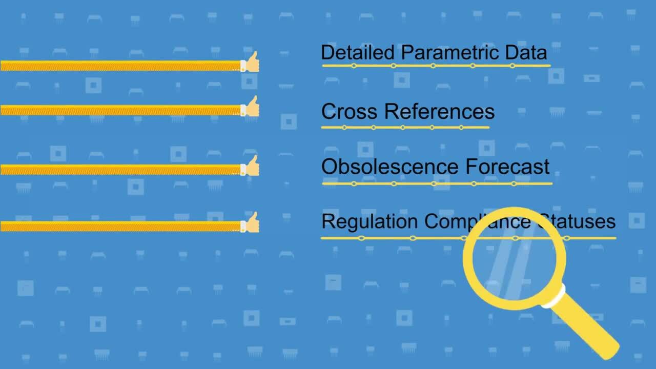
Note: For selected components, LiveBOM also shows:

  • General part information including manufacturer, manufacturer part number, a description, and the category. If available, a link to the datasheet is provided.
  • REACH/RoHS Compliance
  • Status
  • A plot of the market availability score over time
  • A minimum and maximum price for over a set time period
  • Number of vendors with inventory
  • A plot of the vendors with inventory over time
  • Component-specific properties

Step 10: No alternate parts are listed. Select Search to search for an alternate part.

Step 11: Enter Crystal 16MHz into the search field and press Enter.

Replacing Part Numbers in LiveBOM

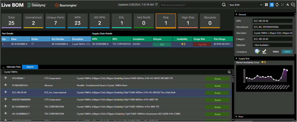
Step 12: Select an available crystal from the listed parts that is reported as low risk. The properties panel shows a higher availability score and more distributors carrying the part.

Step 13: Select the plus sign for Replace MPN to replace the part number. The MPN columns are populated with the part information.

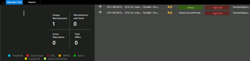
Step 14: View the now-populated alternate parts list and the associated risk.

Synchronizing LiveBOM and the Schematic

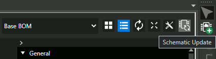
Step 15: Select Schematic Update at the top of LiveBOM. This will change the part number in the schematic.

Note: The part value and footprint will need to be updated manually to reflect the part changes.

Correcting Unmatched Parts in LiveBOM

Step 16: Two capacitors in this design do not have manufacturer part numbers and therefore cannot be analyzed by LiveBOM. Select the No MPN button from the top.

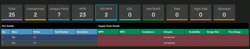
Step 17: View the list of components. All columns from MPN onward are listed as “Unmatched.”

Step 18: Select C3 (22pF capacitor).

Step 19: Enter 22pF into the Search field and press Enter.

Replacing Part Numbers in the Schematic for LiveBOM

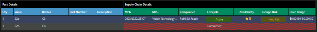
Step 20: Select the first listing of a 22pF capacitor with footprint 0603. Select the plus sign for Replace MPN to replace the part number. The MPN columns are populated with the part information.

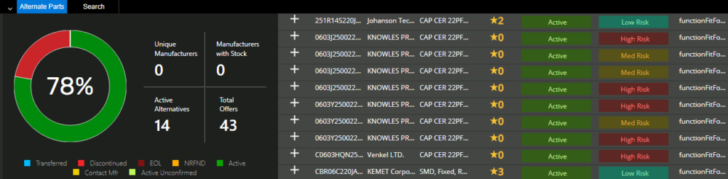
Alternate parts are now listed. If any manufacturers list the part as discontinued or EOL (end of life), different colors are shown in the pie chart.

Step 21: Select Schematic Update at the top of LiveBOM.

Correcting Unmatched Parts in the Schematic

Note: Part numbers can also be modified within the and synchronized with LiveBOM.

Step 22: Select the tab for the schematic.

Step 23: In the project hierarchy, right-click on the .dsn and select Edit Object Properties.

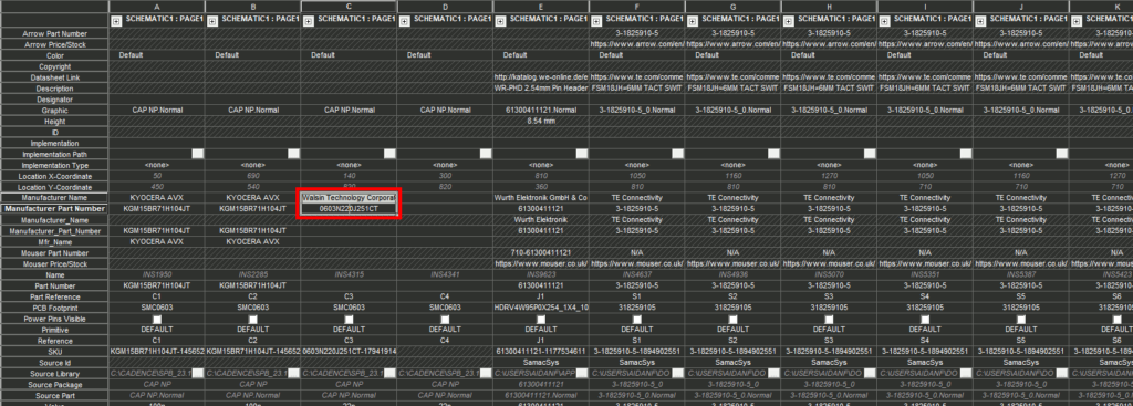
Step 24: Locate C3. The Manufacturer and Manufacturer Part Number fields have been updated to reflect the part change. Hold Shift and select the cells for Manufacturer Name and Manufacturer Part Number for C3.

Copying the Part Information in OrCAD

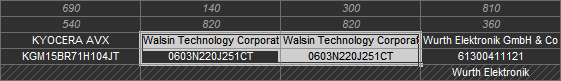
Step 25: Click and drag to extend the manufacturer name and part number into the columns for C4.

Note: This can also be achieved by using CTRL+C and CTRL+V to copy and paste the information within the Properties window.

Step 26: Click Apply and close the Property Editor tab.

Step 27: With the design file selected in the Project Manager, select File > Save from the menu.

Step 28: In the LiveBOM tab, select Total to return to the full component list.

Refreshing the LiveBOM

Step 29: Select Refresh to refresh the BOM. C3 and C4 are now listed with their part numbers.

Note: Repeat this process as needed with other unmatched components.

Wrap Up & Next Steps

Use LiveBOM in OrCAD X to quickly analyze supply chain risk, find suitable alternate parts, and guarantee purchasable components for your PCB designs. Test out this feature and more with a free trial of OrCAD. Want to learn more about OrCAD X? Get access to free how-tos, courses, and walk-throughs at EMA Academy.

Posted on

Electronic Design For Reliability Simulations

electronic design for reliability

electronic design for reliabilityDesigning many electronic products is a complex interplay of mechanical and electrical data, but an additional performance wrinkle is how, not if, a system operates. Simple consumer devices have little stakes if performance is intermittent, but the same is not valid for electronics in medical devices or aerospace. Electronic design for reliability requires an all-encompassing prodding and probing of a device across typical operating conditions to assure uninhibited performance during its useful service life and how failure modes tend to propagate.

ENVIRONMENTAL OUTCOMES AFFECTING ELECTRONIC DESIGN FOR RELIABILITY

Parameter

Environmental Outcome

High temperature

Thermal aging (oxidation, increase in reactivity), thermal expansion

Low temperature

Ice formation, embrittlement, thermal contraction

High humidity

Moisture absorption, corrosion

Low humidity

Embrittlement

Pressure

Outgassing

Debris

Abrasion, clogging

Breaking Down Electronic Design for Reliability

Reliability is perhaps the most overlooked aspect of electronics design from the consumer end – users want their devices to work consistently and with minimal interruptions to operations. Few things are more frustrating than trying to isolate/correct a reliability issue, as interim functionality can greatly impede diagnosis attempts. Crucially, the cornerstone of design for reliability (DFR) is when failure occurs, not if. 

Maximizing the mean time before failure (MTBF) – the goal of any DFR – requires device failure analysis to build resilience and redundancy. For critical devices, industry standards like ISO 13485 and AS9100 provide requirements for establishing and maintaining quality management systems (QMS) to monitor and improve electronic product reliability, for medical devices and aerospace products, respectively. QMSs, which typically include risk analysis plans for specific components and subcircuits, must be adopted and adhered to by both contract manufacturers (CMs), PCB designers and engineers. For the best MTBF rate–a lifecycle estimation based on the total operation time divided by number of failures–reliability simulations during design should be performed.

While the bulk of electronics design focuses on the circuit parameters, the mechanical and thermal aspects of the assembly, wiring harness, and enclosure are also critical to device performance. Design for reliability simulations focuses on these aspects individually and offers insight as to how and where devices are likely to fail under normal operating conditions:

  • Electrical stress analysis – An invaluable tool due to its ability to operate from the schematic, ESAs can diagnose some logic errors based on passive component values and cross-referenced component specifications. Additionally, ESAs perform power analysis to determine thermal dissipation across the circuit. Running these tests pre-layout allows engineers ample time to correct and re-spec component parameters to eliminate errors and minimize thermal effects.
  • Stress derating – Electrical and thermal performance intertwine due to changes in bulk material properties with temperature changes – even though a component may rate acceptably for operation at a specific temperature, its capabilities tend to diminish as temperature increases. Manufacturers’ datasheet information may provide ratings by device temperature, but device and ambient temperature are usually a considerable gap. Designers can use the derating slopes of various components to see if their component values fall within the device ratings or work backward to determine a component that will meet the circuit goals.
  • Thermal analysis – A comprehensive case, substrate, and junction temperature analysis determines hot spots where thermal buildup could cause impedance issues or material aging/damage. In general, high-power and continuously operating elements experience degradation quickly due to the lifetime accumulation of thermal stresses.
  • Shock and vibration analysis – Devices, especially portables or noisy mechanical environments, can experience loss of functionality or degraded service life as solder joints and mechanically coupled connectors wear down.
  • MTBF analysis- MTBF analysis simulates the electrical stress on a circuit by incorporating the intended environment, target PCB life, and the required industry or military standard. Performing MTBF analysis will allow you to evaluate failure in time and the estimated PCB life to identify overstressed components and improve design reliability and longevity. 

These results form an overall reliability prediction that guides schematic- or board-level revisions.

Improving DFR Test Methodology

Electronic reliability follows a general manufacturing trend known as the bathtub curve: early service life failure is due to test escapes (defective devices that elude detection), and the latter service life failures occur as built-up electrical stress alters or reduces component functionality. Between these regions, the incidence of failure is a low (ideally zero) rate of occurrence, provided the device is operating within parameters defined as safe by the manufacturer. There is a reasonable likelihood that devices failing during their useful life may be experiencing thermal overstress conditions that degrade components faster than expected – i.e., the device is exceeding max restrictions or operating at/above safe recommended ratings.

To better identify defects and their vectors, simulations use two general approaches:

  1. Simulations calculate evolving circuit characteristics owing to stress accumulation to determine if the device meets specifications at its indicated end-of-life. More rigorous and comprehensive modeling of electrical characteristics like hot carrier injection and bias temperature instability are necessary to flesh out the aging process of solid-state components. With the continued miniaturization of transistors, modeling must also encompass the 3D shape to accurately capture the interplay between stressors and material aging.
  2. Safe operating checks perform regular checks during simulations and issue warnings when circuit parameters exceed some manufacturers’ listed ratings (e.g., breakdown voltage). Since these checks look for unsafe changes in device characteristics, they can also indicate acceptable changes in performance that function as a measure of reliability. These checks are helpful as they occur during standard pre-layout simulation but have limited scope for end-of-life device fitness.

Standard environmental stress tests may not provide the necessary aging profile for products with a wide range of operating environments, resulting in overly corrective measures to address extreme cases. Consider a device operating with semi-frequent (but not continuous) use over many years: it’s likely to experience extreme high and low temperatures (as well as moisture, debris, etc.) but only for bursts of time. A better DFR profile attempts to randomize both the environmental conditions and duration of each to match the simulation to real-world situations.

EMA Offers Industry-Leading Design Tools

Ultimately, electronic design for reliability depends on the scope outlined in the devices’ goals devised at the outset of design: The more intense the need for uninterrupted uptime and performance, the more stringent the simulations necessary to properly model the long-term device behavior. EMA Design Automation provides software programs and integrations that enable you to perform electrical stress analysis and MTBF simulations to ensure your design achieves your performance and operational lifecycle objectives.

EMA Design Automation is a leading provider of the resources that engineers rely on to accelerate innovation. We provide solutions that include PCB design and analysis packages, custom integration software, engineering expertise, and a comprehensive academy of learning and training materials, which enable you to create more efficiently. For more information on electronic design for reliability and how we can help you or your team innovate faster, contact us.


Posted on

Power MOSFET SPICE Model: Explained


Modeling designs helps engineers verify whether their circuit will function as intended. Modeling programs simulate circuit behavior under different conditions and in accordance with the design requirements, allowing engineers to better plan and build circuits.

Typically, to model components, generic models are used, which produce inaccurate and unrealistic simulations based on ideal conditions. This can cause functionality issues to go undetected until far later in the design process. To confidently simulate a component, create a Power MOSFET SPICE model using specifications from a manufacturer’s datasheet.

What is a Power MOSFET?

A Power Metal Oxide Semiconductor Field Effect Transistor (MOSFET) is a voltage-controlled device used to switch large amounts of current. Power MOSFETs are frequently used due to their low-gate drive power and fast switching speeds.

What is Needed to Model a Power MOSFET?

To create the required Power MOSFET for simulation, two items must be defined:

  • Type
    • What type of MOSFET is required: N-Channel or P-Channel?
  • Power MOSFET Characteristics
    • What are the required parameters for the Power MOSFET: input/output capacitance, diode forward voltage, total gate charge, etc.?

This information must be incorporated into the SPICE simulation model which can be achieved by manually creating or editing a text file. Keep in mind if the model created does not produce the intended outcome or if a part is changed, values will need to be edited manually. This manual process to produce the desired model is time consuming and increases the likelihood of errors; however, the PSpice Modeling App provides a fast, easily-configurable, and fully-integrated method to create a Power MOSFET SPICE Model for simulation.

Creating a Power MOSFET SPICE Model with PSpice

The Power MOSFET modeling application quickly creates Power MOSFET models with a wizard-based approach. The parameterized MOSFET enables simulation and testing of the model in various conditions. The necessary specifications are predefined and users can easily input the Power MOSFET characteristics, defined by manufacturers, directly into the parameters:

Datasheet Parameters for Power MOSFET SPICE Model Creation

  • Type:

Select either N-Channel or P-Channel.

  • Reverse Transfer Capacitance:

Define the small-signal reverse transfer capacitance (Crss). This value must be between 0nF and 10nF for both N-Channel and P-Channel MOSFETs.

  • Input Capacitance:

Define the small-signal input capacitance when the drain and source terminals are shorted (Ciss). This value must be between 0nF and 10nF for both N-Channel and P-Channel MOSFETs.

  • Output Capacitance:

Define the small-signal output capacitance when the gate and source terminals are shorted (Coss). This value must be between 0nF and 10nF for both N-Channel and P-Channel MOSFETs.

  • Drain-to-Source Voltage:

Define the maximum drain-to-source voltage the device can sustain when in the off state (BVDss). This value must be between 1V and 1kV for N-Channel MOSFETS or between -1V and -1kV for P-Channel MOSFETs.

  • Drain-to-Source On-Resistance:

Define the electrical resistance when the device is in the on-state. The drain-to-source on-resistance (RdsON) value must be between 1n ohms and 100 ohms for both N-Channel and P-Channel MOSFETs.

  • Series Gate Resistance:

Define the Series Gate Resistance (Rg). The gate resistance is caused by the resistance of the gate conductors as well as the metal and contact structures that route the gate signal to the pad for external package connection. This value must be between 1n ohms and 100 ohms for both N-Channel and P-Channel MOSFETs.

Creating a Power MOSFET SPICE Model with the PSpice Modeling Application
Power MOSFET SPICE Model Creation in PSpice

  • Gate-to-Source Threshold Voltage:

Define the minimum gate bias which can form a conducting channel between the source and drain. The gate-to-source threshold voltage (Vgs_th) value must be between 1nV and 10V for N-Channel MOSFETs or -1nV and -10V for P-Channel MOSFETs.

  • Diode Forward Voltage:

Define the forward voltage drop of the integral body diode when a set current is applied to the source. The diode forward voltage (VSD) value must be between .3V and 1V for N-Channel MOSFETs or -.3nV and -1V for P-Channel MOSFETs.

  • Drain-to-Source Leakage Current:

Define the leakage current flowing between the source and the drain. The drain-to-source leakage current (Idss) value must be between 1pA and 1mA for both N-Channel and P-Channel MOSFETs.

  • Total Gate Charge:

Define the amount of charge required for the gate driver to turn the device on or off itself. The total gate charge (QG) value must be between 1pC and 100uC for both N-Channel and P-Channel MOSFETs.

  • Voltage for Specified Total Gate Charge:

Define the voltage for the specified total gate charge (V_QG). This value must be between 1uV and 10kV for N-Channel MOSFETs or -1uV and -10kV for P-Channel MOSFETs.

  • Forward Trans-Conductance:

Define the gain of the MOSFET or the ratio between the change in Ids and change in Vds. The forward trans-conductance (GFS) value must be between 1mS and 1e5S for both N-Channel and P-Channel MOSFETs.

  • Body Diode Reverse Recovery Time:

Define the time it takes for the stored minority charges to be removed, passively or actively, when the diode switches from the on-state to the off-state. The body diode reverse recovery time (Trr) value must be between 0s and 1s for both N-Channel and P-Channel MOSFETs.

Using the inputted information above, the PSpice Modeling App generates a schematic symbol and automatically associates the newly created Power MOSFET SPICE model without leaving the OrCAD Capture environment. The PSpice Modeling App also automatically manages the simulation profile configuration, eliminating any library set up for simulation.

To try this yourself, be sure to download the Free Trial of OrCAD. Check back for additional SPICE model how-tos and get step-by-step instructions to create a Power MOSFET SPICE model in PSpice here.

Posted on

EMA Makes OrCAD CIS & CIP Training for Library & Component Management Free for Everyone

OrCAD Capture CIS and CIP Training

To celebrate the launch of OrCAD X and the fact that Cadence has included the very popular CIS option in their new OrCAD X PCB design suites we have decided to make our training course free to help customers leverage this new technology as they begin to adopt OrCAD X.

If that’s all you need to know you can access the free course here: OrCAD Capture CIS and CIP Training | EMA Design Automation (ema-eda.com) (just need to register…which is also free)

If you are looking for more information about what OrCAD CIS and CIP are and what they do for you read on…

What is CIS & CIP?

OrCAD CIS and OrCAD CIP stand for Component Information System and Component Information Portal respectively. What they do is enable your OrCAD environment to store, source, and manage your part library leveraging a relational database. This provides several significant benefits.

CIS enables the ability to connect OrCAD to a database which allows you to:

  • Integrate and centralize your component data
  • Provide parametric part search capabilities
  • Preview symbols and footprints before use
  • Templatize and configure BOM generation
  • Integrate part management
  • Support design variants

CIP provides the means of populating, managing, and automating this database so you can leverage it to the fullest including:

  • Search and import distributor parametric data for your parts (as well as keep this data updated automatically)
  • Connect supply chain data such as lifecycle, risk, cost, and compliance so you can easily make supply chain driven part decisions
  • Integrate with CAD library services such as Ultra Librarian to eliminate the need to build CAD models
  • Track changes to part status and other key metrics and trigger notifications off these changes
  • Identify multiple sources for parts to ensure availability
  • Leverage functions like ‘where used’ to quickly see the impact of part changes across all your designs (past and present)
  • Manage users and roles to ensure data integrity and traceability

As you can see this is quite a powerful combination providing comprehensive part and library management capabilities directly inside the OrCAD design environment. These new capabilities mean there are now new ways to access and leverage your parts that you may not have been used to in OrCAD.

The OrCAD CIS and CIP training will help users get acclimated quickly to how to leverage these tools to their fullest.

Why Are We Making This Course Free?

This course was originally created based on requests from customers who had chosen to adopt this managed library flow. While this course has been available for a while, it was only applicable to those that owned these options for their OrCAD software. With CIS being made a part of the standard OrCAD X suite configurations this meant a lot more users were about to get access to this way of managing their libraries and data and we wanted to make sure this was a smooth transition for all users. Making this course free will (we hope) help users adopt CIS and the managed library approach which we have seen through years of experience means a more efficient and effective design process, and a happier customer.

How to Access the OrCAD CIS and CIP Training?

If you didn’t see above, the OrCAD CIS and CIP training course is part of the EMA Academy and is available to all users who have an active account (which is free) or who register for one. If you need to you can register right on the course page itself, just select login to enroll and complete the quick registration process.

Login and Register for the OrCAD Capture CIS and CIP Training

We hope customers will take advantage of this free training opportunity to help them learn how to leverage one of the key new features in the OrCAD X release.

OrCAD Capture and OrCAD Capture CIS

OrCAD Capture

Industry leading schematic capture environment for first pass success

Limitless Schematic Design

Hierarchical Design Support

Large Pre-Built Library

Component Management

Complex Rule Support

Integrated Simulation

Design Variants

Intelligent PDF Output

Comprehensive Schematic Design at Your Fingertips

Shorten your product design cycle with embedded rules, seamless PCB and simulation integration, automated design rule checks, and an integrated component library directly within your schematic canvas.

Electronic Rules Check
and Embedded Rules

Easily define and embed design rules in the schematic to drive the PCB layout and clearly communicate vital functionality requirements. The customizable ERC Matrix allows for easy definition of errors and warnings when testing connections between pins, hierarchical blocks, and hierarchical ports. Verify schematic accuracy with real-time design rule checks for common electrical, physical, and simulation errors.

Productivity-Focused
Environment

Efficiently create designs from simple block diagrams to complex hierarchical, multi-sheet schematics with OrCAD’s comprehensive design environment. Work at peak efficiency with automated design cache for recently used components, reference designator assignment, annotation, and back annotation. Designed with your preferences in mind, OrCAD’s customizable workspace and toolbars along with its open design framework, TCL scripting, and app support, create an easily configurable user experience.

Expansive Component Library

Design efficiently with a standard library of commonly used schematic symbols including power, ground, off-page connectors, no connects, hierarchical blocks, and ports. Easily select parts from an extensive library of commonly used components including discretes, FPGAs, Opamps, Microcontrollers, and more. With integration to Samacsys and Ultra Librarian, easily view live parametric data for millions of components and quickly incorporate verified symbols, footprints, and 3D models into your design. Direct connection to your component database within the schematic canvas guarantees company-approved parts are selected for designs.

Clear and Accurate Reporting

Streamline design reviews with an intelligent PDF of the schematic and interactive identification of components, nets, connectivity, and more. Guarantee component purchasing and assembly with customizable component properties and Bill of Material creation. Accelerate BOM creation with predefined properties, templates, and automatic population of information directly from your component database to create zero-touch BOMs.

Seamless PCB and Simulation Integration

Seamlessly communicate design intent with one-click netlisting and PCB creation. Confidently pass information between the schematic and PCB with bi-directional publishing and automatic identification of changes. Perform early analysis on your critical high speed nets with built in signal integrity analysis. With integrated access to PSpice, easily simulate circuit behavior directly within the schematic; no design translations necessary.

Variant Support

Easily support world-wide production and manage component variations for multiple manufacturing and design requirements with OrCAD. Define differing component values or do not stuff components and efficiently communicate assembly changes with color-coded schematic information, variant bill of materials, and variant reports.
Streamlined Schematic Entry
Hierarchical and Multi-Sheet Schematics
Block Diagram Support
Snap Functions and Grids
Efficient Connectivity and Automatic Wiring
Automated Component Alignment and Distribution
Differential Pair Definition and Management
Graphical Design Compare
Comprehensive Project Hierarchy
Customizable Workspace and Open Design Framework
Automatic Titleblocks
Automated Design Cache
Comprehensive Schematic Search and Bookmarks
Picture and Documentation Support
Built-in Translators (Altium, Mentor, Eagle, more)
Integrated Access to Component Database
Integrated Part Manager
Part Status Notificaition
Design Variant Support
Color-Coded Variant Component Display
Libraries, Symbols, and Models
Schematic Symbol Editor
Library of Common Schematic Symbols
Library of Common Components
Millions of Symbols, Footprints, and 3D Models
Customizable Component Properties
Easy Association of Supporting Models
Centralized Component Data
Parametric Part Search
Temporary Part Management
Symbol and Footprint Preview
Streamlined Temporary Part Creation
With CIP
Easy New Part Introduction
With CIP
Automatic Population of Parametric Information
With CIP
Automatic Part numbers
With CIP
Part History
With CIP
Association of Simulation Models, Symbols, Footprints, Datasheets, and Documents
With CIP
Starter Component Database Schema
With CIP
5,000 Part Starter Database
With CIP
Bulk Import of Existing Components
With CIP
Access to Component Database Through Web Browser or OrCAD
With CIP
Streamlined Component Searches
With CIP
Customizable Permissions for Component Library
With CIP
Supply Chain Insights
Real-Time Pricing and Availability
With CIP
Real-Time Compliance Based Search
With CIP
Multi-Sourcing Support
With CIP
Integrated Distributor Information (Digi-Key, Mouser, Arrow, and More)
With CIP
Where-Used
With CIP
Cloud Enabled Services
Cloud-Based Workspaces
Managed User Roles
Customizable Permissions
File Management and Version Control
Integrated Part Authoring and Management
Promoted Library of Symbols and Footprints
Automatic Population of Parametric Information
Association of Simulation Models, Symbols, Footprints, and Datasheets
Comprehensive Rules and Checks
Electrical Design Checks
Physical Design Checks
Simulation Design Checks
Custom Design Checks
Customizable ERC Matrix
Define Design Check Exemptions
Real-Time Design Rule Checking
Embedded Rules
Net Property Definition and Management
Electrical Rule Definition and Management
Physical Rule Definition and Management
Spacing Rule Definition and Management
Streamlined Integration
PCB Layout Creation and Automatic Netlist Generation within your Schematic
Real-Time Design Synchronization
ECO Support
Cross Probing and Cross Placement of Components Between Schematic and PCB
Integrated Spice Simulation
Signal Integrity Simulation
Accurate Reporting
Standard PDF Output of the Schematic
Intelligent PDF Output of Schematic
Automatic Netlist Generation
Customizable Bill of Material (BOM)
Automated Zero-Touch Bill of Material (BOM) Creation
BOM Templates
Relational BOM Support
BOM Variant Support
Variant Report
Easy BOM Import/Export
With CIP
Easy BOM Revisioning
With CIP

Get the Most Our of Your Schematic Design Tool

Get the most out of OrCAD Capture with these additional integrations. OrCAD Capture Component Information Portal (CIP) simplifies part management and selection with an easy-to-use interface integrated directly within OrCAD Capture. OrCAD Engineering Data Management (EDM) allows you to manage all aspects of your design data and ensure seamless team collaboration with features such as revision control and library management. Get control over the supply chain with access to critical part information and identify unorderable, obsolete, and high-risk parts directly in the schematic using SE Connect BOM Risk. Constraint Design EE effortlessly manages your high-speed PCB Design rules at the schematic level.

OrCAD PCB Designer

See how OrCAD PCB Designer seamlessly integrates OrCAD Capture and PCB Layout for the ultimate design experience

OrCAD PSpice Designer

Learn how OrCAD PSpice Designer can easily verify schematic functionality directly with OrCAD Capture.

SCHEDULE A DEMO

Posted on

What is OrCAD X Capture CIS?

OrCAD X Capture is a well-known, industry standard software solution boasting limitless schematic design capabilities and expansive functionality to accurately document electronic design intent. OrCAD X Capture has a variation referred to as OrCAD X Capture CIS which now comes standard in the OrCAD X PCB design suites. But what is CIS and how does it differ from the typical OrCAD X Capture design environment? Whether you have upgraded to OrCAD X or are new to OrCAD X Capture CIS, let’s take a look at what exactly OrCAD “CIS” is, so you can leverage the additional functionality throughout your PCB design process.

What is OrCAD CIS?

OrCAD X Capture CIS

 CIS stands for the Component Information System. In addition to the standard OrCAD X Capture functionality for schematic designs, CIS provides a database connection. With CIS, you can achieve a link between your component database and your ECAD design environment. By establishing this link, you can source components from a centralized repository and synchronize designs with your component library to ensure up to date component information.

Key Features of OrCAD X Capture CIS

By incorporating the Component Information System (CIS) into your OrCAD X Capture design environment, additional features and capabilities can be leveraged when creating your schematic:

    • Integrated, Centralized Component Data
    • Obtain direct access to shared, centralized component data containing company approved symbol and footprint libraries within the schematic canvas.

    • Parametric Part Search
    • Search your component database based on parametric information to quickly find the desired part for your designs.

    • Symbol and Footprint Preview
    • View the corresponding symbol and footprint before placing a database part in your schematic design.

    • Efficient BOM Generation
    • Quickly create BOMs with predefined properties and automatic population of information based on your component database to create ready-to-order BOMs. Create templates to accelerate the BOM creation process and include multiple distributor options to ensure efficient purchasing and timely sourcing.

    • Integrated Part Manager
    • Ensure parts used in the schematic are up to date with an easy real-time status check of all components used in the design. A configurable color-coded status identifies components that are approved, temporary, and more directly in the schematic.  

    •  
    • Design Variant Support

      Create a design variant by defining differing component values and do not stuff components. CIS contains variant reporting to automatically generate a report including component differences between a core design and a variation as well as BOM Variant Support to easily select which design variation should be used to create the Bill of Materials.

    Utilizing these key features during schematic creation results in several benefits to your PCB design process.

    Benefits of OrCAD X Capture CIS

    The ability to access a component data management system within your ECAD design environment provides designers with an efficient method to use verified and approved components for their designs. This alone has an immense impact on the speed and accuracy of documenting your electronic design intent. In addition, the features and capabilities of OrCAD X Capture CIS improve your design process by:

      1. Creating Consistency

        Without a component database, typically users manage parts on individual machines or shared servers. With CIS, all team members are pulling component data from a centralized database of approved parts, creating consistency and reducing errors. The integrated part manager ensures data remains consistent between your design and the component database with seamless synchronization.

      2. Saving Time

      •  
      • With a component data management system, each user isn’t responsible for the creation and management of parts. This reduces duplicate efforts for creating the same parts, symbols, and footprints as well as reduces the time spent verifying component data.
      •  

      3. Making Informed Part Decisions

        Centralized component data, part parametric search capabilities, as well as a symbol and footprint preview allow designers to review all component information up front within their CAD environment to quickly select the best component for the design.

    Achieving a streamlined design environment with OrCAD X Capture CIS can greatly improve team collaboration and your PCB design process; however, there are some considerations and questions you need to ask yourself to configure a component data management system that sets your team up for success. 

    Component Database Considerations

    To implement a component data management system that can fully realize the benefits of OrCAD X Capture CIS, there are some questions that must be considered:

      • How do you setup your database?

      • How do you determine and implement a database schema?

      • How do you determine and implement a part number scheme?

      • How do you map existing symbols and footprints to components and parametric data?

      • How do you update the information found in your component database?

      • How do you manage alternate manufacturers or distributors?

      • How do you ensure data integrity?

    These questions must be addressed to develop a plan for successfully implementing and managing PCB component data. If the above questions are not considered upfront, managing the contents of your database may be problematic- this is where OrCAD Component Information Portal (CIP) can help.

    Efficiently Managing Component Data with OrCAD CIP

    CIP Flow Diagram


    Component Data Management with OrCAD CIP


    The benefits of OrCAD X Capture CIS can be easily realized and enhanced with the addition of OrCAD Component Information Portal (CIP). OrCAD CIP provides an easy-to-use interface and database management tools to populate and update your component database. OrCAD CIP fulfills many component database considerations to achieve a comprehensive component data management solution with:

        • Starter Component Database Schema and 5,000 Part Starter Library

        • Automatic Part Numbers

        • Automatic Population of Parametric Information

        • Detailed Part History

        • Bulk Import of Existing Components

        • Real-Time Pricing, Availability, and Compliance Information

        • BOM Import/Export and Revisioning

      By incorporating OrCAD CIP into your OrCAD X Capture CIS environment, you can accelerate component database creation and enhance your component data management system. See how the functionality of OrCAD CIP can streamline your PCB design process here.

      Posted on

      Real-Time Part Management with OrCAD Capture CIS

      Keeping the schematic in sync with the part database can be a tedious, time-consuming task. OrCAD Capture CIS streamlines this process with:

      • Real-time part information
      • Color-coded part status
      • Automatic synchronization of the schematic and component database
      • Automatic identification of component differences
      • Color-coded components on the schematic and component database

      Efficiently manage parts for your PCB designs and ensure schematics are up-to-date with accurate component information with real-time part management in OrCAD Capture CIS.

      SiliconExpert – Electronic Component Database

      SiliconExpert

      Comprehensive supply chain data for millions of devices.

      Request Info

      Make Better Part Decisions, Faster

      Ensure your parts will be correct, available, and in compliance with access to deep data insights available across 300+ million parts from 15,000+ suppliers. SiliconExpert allows product teams to:

      • Mitigate risk with advanced lifecycle, sourcing, and environmental compliance data
      • Avoid late-stage redesigns with proactive PCN notifications and form-fit-function cross references
      • Save time with access to a single, comprehensive parts database with all the information you need to make intelligent part selection decisions

      Capabilities

      300+ Million Parts

      Access up-to-date data for millions of electronic parts using partial part numbers or description searches.

      Comprehensive Compliance Data

      Quickly determine if parts will meet your environment and regulatory compliance requirements for directives such as RoHS & REACH.

      Part Lifecycle and Risk Analysis

      Learn upfront if new parts are in line with your product lifecycle and manufacturing yield objectives. Gain insight into obsolescence and counterfeit risk using advanced lifecycle algorithms.

      Cross References

      Easily identify form-fit-function replacements for parts to eliminate costly re-designs and ensure product delivery schedules are met on time. 

      BOM Management

      Comprehensive BOM scrubbing and management tools ensure there are no surprises when moving to production.

      Seamless Integration

      Easily connect SiliconExpert part data with your internal systems using the robust API. 

      Subscription Options

      Just need access to part data or want to dynamically manage your Bill of Materials?

      Choose the subscription option that best meets your needs.

      Part Search

      Unlimited Access to Part Data

      • Search 300+ million components
      • Parametric search
      • Cross reference
      • Lifecycle status
      • Inventory risk
      • Regulation compliance data
      • Country of origin data
      • Datasheet history
      • Export
      • Forecast years to end of life
      • Side by side part comparison
      BOM Manager

      Complete Part and BOM Management and Analysis

      Everything in Part Search, plus:
      • Scrub and manage bill of materials
      • Bill of material grading
      • Advanced reporting
      • Part change alerts
      • Normalize internal part numbers
      • Upload & apply AML/AVL lists

      Use OrCAD?

      Enable supply chain driven part selection with access to SiliconExpert

      data directly inside your OrCAD design envinronment.

      CIP Compliance Module

      Get A Quote

      Find the version and licensing agreement that best fits your needs and budget.

      Request Quote

      Customers Include


      "Our Component Engineers were able to use the tool to find a replacement component with improved characteristics, a smaller package, lower cost, a longer lifecycle and readily available stock. This search could have potentially spanned one of multiple weeks through phone conversations, publication reviews and internet searches. But because of SiliconExpert's tools, we were able to complete this step in a significantly shorter time span."


      John Starr

      Component Engineer

      Intermec, Inc

      Free Trial

      See what your parts aren't telling you. Get access to the largest and most accurate part information database and solve your electronic component supply chain issues before they happen. 

      Request Trial

      Need more info?

      The EMA Team will be happy to assist you.

      Contact Us

      How to Utilize Where Used Functionality in OrCAD CIP

      Many of today’s electronic products leverage a company’s intellectual property, reusing known-good circuits and making modifications to accelerate the design process; however, with fluctuations in the supply chain and a rapid component lifecycle, ensuring all the components needed are available and purchasable can be time-consuming. With Where Used functionality in OrCAD CIP, you can easily identify every design a component is used in to easily identify and replace unavailable components.

      This quick how-to will provide step-by-step instructions on how to use where used functionality in OrCAD CIP.

      How-To Video


      Open in New Window

      Uploading a Bill of Materials

      Step 1: Open the desired design in OrCAD X Capture CIS.

      Note: The selected design must be completed with components found in your component database.

      Step 2: Select CIP > Open CIP from the menu. If prompted, login with your username and password.

      Step 3: To track where parts are used, Bills of Materials (BOMs) for projects must be uploaded. In CIP, select BOM > View/Import from the menu.

      Step 4: Select the + icon to add a new BOM in CIP.

      BOM Management in OrCAD CIP

      Step 5: Add a Part Number for the BOM or select the auto-generate icon to fill in the field with the next available BOM number.

      Step 6: Add a Revision for the BOM and any other desired information.

      Step 7: Select the + icon to add the BOM with the defined part number.

      Creating a BOM in OrCAD CIP

      Step 8: Select Delimited for the BOM view. This will display a BOM with each part number shown on a single line where reference designators are shown as a comma separated list.

      Note: Other BOM view options include:

      • Single: Each reference designator is shown on a single line.
      • Compact:  Each part number is shown on a single line where reference designators are shown as ranges or a comma separated list.

      BOM views can be configured before or after import.

      Step 9: In this interface you have the option to import the BOM from a CSV file or use a design. Select Import from DSN.

      Step 10: The opened design is automatically selected in the BOM Import window. Select Import BOM.

      Note: To successfully import a BOM from a design, all components must be found in your component database.

      Importing a BOM in OrCAD CIP

      Step 11: When BOM Import is complete, a pop-up window will appear. Click OK to close the window.

      Identifying Obsolete Components

      Step 12: Select CIS DB Search from the main CIP menu.

      Configuring a Database Search in OrCAD CIP

      Step 13: Select the drop-down list for Parametric Field and select Company Part Status.

      Note: This can also be configured to search Manufacturer Part Number Status by selection Manufacturer PN Status from the Parametric Field drop-down list.

      Step 14: Ensure Contains is selected as the Operator.

      Step 15: In the Parameter field enter Obsolete.

      Note: Additional search fields can be configured by selecting the + under the Add/Remove column.

      Step 16: Select Search. The search returns any components listed as Obsolete within the Company Part Status field.

      Where Used Functionality in OrCAD CIP

      Identifying Obsolete Components in OrCAD CIP

      Step 17: Select the part number for desired component from the search results to view additional details.

      Where used functionality in OrCAD CIP identifies where components are used throughout your designs and BOMs.
      Where Used in OrCAD CIP

      Step 18: If this component is used in any designs, the number of BOMs the component is used in will be visible on the Where Used tab. Select the Where Used tab.

      Note: To utilize the Where Used functionality, BOMs must be imported and managed within CIP.

      Step 19: All designs and BOMs where the component is used are reported. Select the desired BOM Part Number to view the BOM.

      Wrap Up & Next Steps

      Easily identify every instance of a component’s use throughout all your designs with Where Used in OrCAD CIP.  Get more step-by-step instructions for OrCAD CIP at EMA Academy.

      How to Quickly Determine where Obsolete Components are Used

      A centralized component database provides access to verified and approved parts for your entire team; however, when components become obsolete it can be impossible to remember where they were used. Identifying and replacing these obsolete components is vital when reusing intellectual property or creating a new revision of an existing design. With OrCAD Component Information Portal (CIP), you can quickly identify the obsolete components and determine where they were used in your designs with saved searches.

      This how-to provides step-by-step instructions for creating a saved search in OrCAD CIP to determine which designs contain obsolete components.

      How-To Video

      Configuring Database Search

      Step 1: Select CIP > Open CIP from the menu and enter your login information.

      Note: The CIS DB Search tab is automatically opened in the CIP window.

      Identifying Components that are End of Life

      Step 2: Enter the desired search parameters. To identify components that have 0 years until “End of Life,” configure the following parameters:

      • Parametric Field: YearsEOL
      • Operator: Equals (=)
      • Parameter: 0

      Note: The YearsEOL parameter is available for users that have purchased the CIP Compliance Module and estimates the number of years until a component becomes obsolete. Saved searches are fully customizable and can search numerous component parameters including Company Part Status, Values, Manufacturing information, and more.

      Step 3: Select the + under Add/Remove.

      Note: This has automatically added a Condition to the search parameter.

      Adding a Parameter to the Component Database Search

      Step 4: Set the condition to OR.

      Identifying Components that are near the End of Life

      Step 5: Enter another search parameter. To identify components that have 1 year until “End of Life,” configure the following parameters:

      • Parametric Field: YearsEOL
      • Operator: Equals (=)
      • Parameter: 1

      Including Additional Fields

      Step 6: Select Include Additional Fields in Search Results.

      Note: This displays additional parameters within the search results, allowing you to review all relevant information without selecting each individual component.

      Identifying the BOM Where a Component is Used

      Step 7: From the drop-down selection, choose BOM under the Where Used section.

      Note: This will automatically identify the Bill of Materials (if any) where the component is used.

      Step 8: Select the + next to the BOM parameter.

      Step 9: From the drop-down selection, choose Company Part Status.

      Reusing a Component Database Search

      Saving Parameters to Reuse a Component Database Search

      Step 10: Under Save a Search, enter a name for the search.

      Note: Selecting Global will make the search available for all users. If global is not selected, the search will be available locally.

      Step 11: Select Save and close the Search Saved Successfully window.

      Searching for Part Obsolescence

      Step 12: Select Search.

      Searching Database for Obsolete Components

      Step 13: View the search results to identify components that are 0-1 years away from obsolescence and determine where these components are used.

      Identifying BOMs Associated with Obsolete Components

      Note: Selecting a part number will bring you to the component page in the database. Here you can view additional component information as well as the corresponding BOM.

      Reusing Saved Search Parameters

      Step 14: Return to the CIS DB Search tab. The newly saved search is available in the drop-down selection under Select a Search and can be used to expedite future searches.

      Wrap Up & Next Steps

      Easily find desired components in your centralized database with the ability to save custom searches locally or globally in OrCAD CIP. This method helps identify obsolete components and where they are used, allowing you to replace components as needed for future design revisions. For more information and in-depth training on additional features, view our E-Learning and instructor led courses for OrCAD Capture CIS and CIP.

      EMA Design Automation