Posted on

Electronic Product Design Cost: Estimating and Determining ROI


Controlling the electronic product design cost


Bringing a new electronic circuit board to the market is complex and includes several processes and

stages. Depending upon the complexity of the design, development can take weeks or months. Even longer, if you encounter supply chain issues, such as delayed component shipments, manufacturing shortfalls, or obsolescence. Additionally, manufacturing issues can extend the development cycle. Several factors contribute to these major sources of waste. However, with effective electronic product design cost management, you can overcome these challenges and maximize your development ROI.
.

Factors That Drive PCBA Development ROI

PCBA development consists of three distinct but interdependent stages. The fact that design, manufacturing, and testing stages are performed by multiple companies only accentuates the importance of individual optimization and integration between stages. Accomplishing this begins with identifying the important cost factors for development.

PCBA DEVELOPMENT COST DRIVING FACTORS

Development Stage

Cost Factor

Description

Design

Engineering

Includes man-hours for circuit design, component selection, and design verification.

Software Tools

Includes the PCBA design, signal integrity (SI), power integrity (PI), power distribution network (PDN), and thermal and electromagnetic interference (EMI) simulation and analyses.

Manufacturing

Fabrication

Includes board materials, imaging, etching, hole drilling, and solder masking.

Assembly

Includes picking and placing parts, soldering components, and inspections.

Testing

Functional Testing

Includes time domain reflectometry (TDR) and impedance match checking. 

In-Circuit Testing (ICT)

Includes apparatus, such as a flying probe.

Structural Testing

Includes third-party board tests, like HALT/HASS. 

As shown in the table above, every stage of PCBA development directly impacts overall cost and ROI. Once a basic design has been created (including component selection, schematic capture, and PCB layout), most development costs can be fixed. It should also be noted that ICT is not typically needed, especially for IPC Class 1 and many Class 2 applications. Further, structural testing, which often involves destructive testing regimens, is only required for critical industries (defense and aerospace) and hazardous environment board implementations.

EDA software costs are often flexible. This is because circuit analysis, RF, and other simulations and analyses for design verification are not included in most PCBA design packages. Therefore, the effectiveness of electronic product design cost management can significantly influence overall PCBA development costs and ROI.

The Importance of Electronic Product Design Cost Management

Effectively managing the costs for designing your board is important for its direct impact and the design process's effect on the cost for all other stages. Excluding special testing regimens, PCBA design has the following impact on development costs.

Impact of PCBA Design on Development Costs

  • Design Costs
    The costs for designing your board include fixed and variable factors. Your basic EDA program is fixed, but engineering, component selection, and design verification vary according to the project specifications. For example, component availability and other supply chain issues vary greatly from design to design. It is also necessary to ensure that your design meets functional and operational objectives, adheres to industry regulations and standards, and falls within your CM’s DFM and DFA rules and guidelines. These software tool analysis and simulation requirements influence the design and overall development costs.

  • Fabrication Costs
    The PCB fabrication process consists of fixed steps. However, your design decisions can determine exactly how these are performed. For example, the number of layers determines how many substrate-laminate presses are needed. Additionally, your choice of surface mount device (SMD) component packages, number, and type of vias can dictate the type of drill used and how many plated through-holes (PTHs) are required. Other decisions, like solder masks and surface finish types, can also vary in cost.

  • Assembly Costs
    PCB assembly is similar to fabrication because the steps are generally fixed. The exception is for the soldering technique, which is based on types of components. Wave soldering is the most common technique for through-hole parts, which are typically the most costly. However, reflow is used for SMDs. Board cleanings and protection methods such as conformal coating or encapsulation influence costs.

  • Testing Costs
    Manual and optical inspections and some tests, such as automatic optical inspection (AOI), are typically always performed. Other tests, such as TDR, peel (which tests lamination adhesion), Resistivity of Solvent Extract (ROSE), and solder pot and float tests, may not be routine and will often increase the cost.

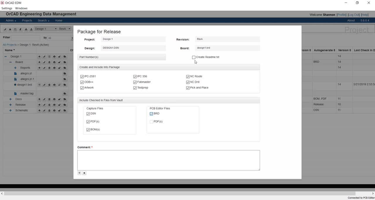
In addition to these specific stage costs, excessive board respins can also increase development costs. These may be largely unavoidable for some highly complex PCBA designs. However, additional board spins are often required to bring the design specifications in line with the DFM and DFA rules and guidelines for your CM’s equipment or to make changes to improve circuit functionality and operation. Additional costs for performance and manufacturability can be significantly reduced or even eliminated by using PCBA design support software tools. 
.

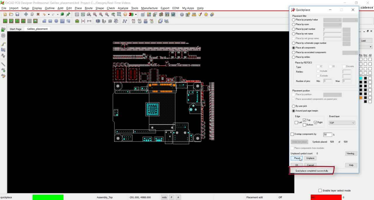
How PCBA Design Support Tools Improve Development ROI

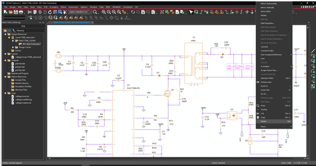
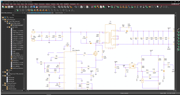
Most PCBA design packages are great for creating schematics and doing PCB layouts. Additionally, most include functionalities to aid engineers and designers, such as constraint management, DRC, auto-routing, and some form of DFM validation. Nevertheless, PCBA design can still be tedious to create a design that meets its operational performance objectives and satisfies your CM’s manufacturability requirements. The additional time, engineering resources necessary, and manufacturing costs can be significant.

Electronic product design and total development costs can be reduced with software development tools. The tools listed below improve the efficiency and accuracy of your design.

Benefits of PCBA Design Support Software Tools

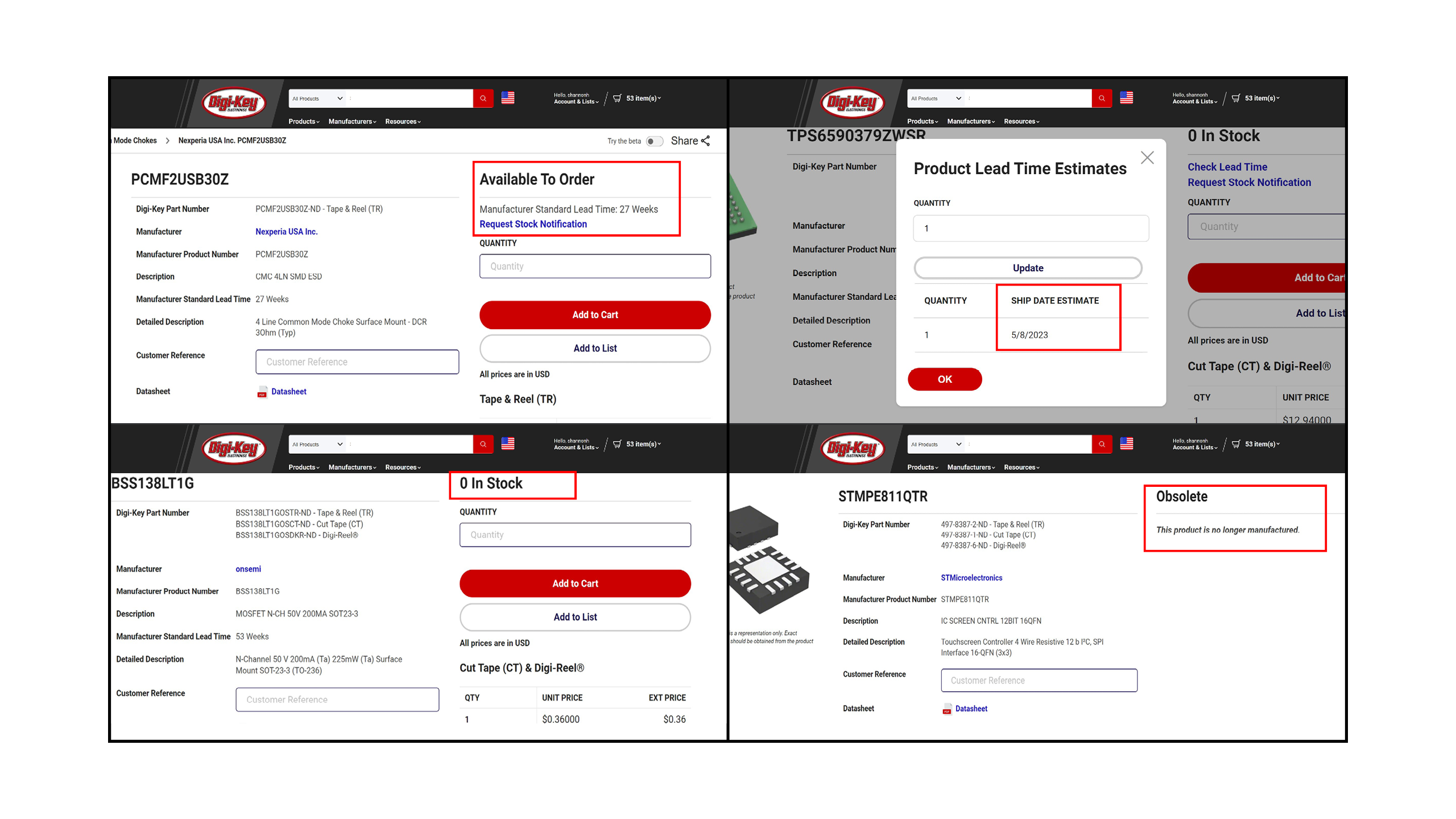
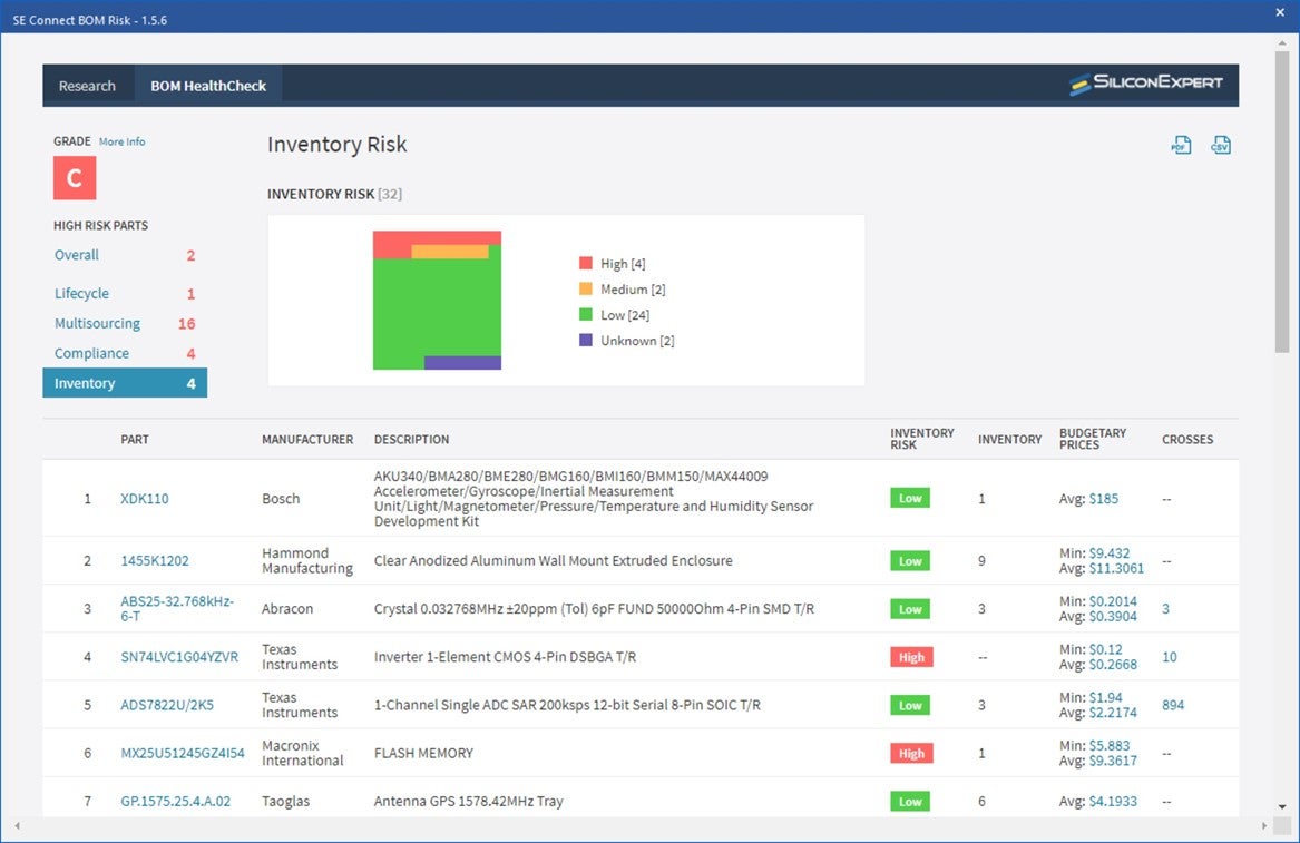
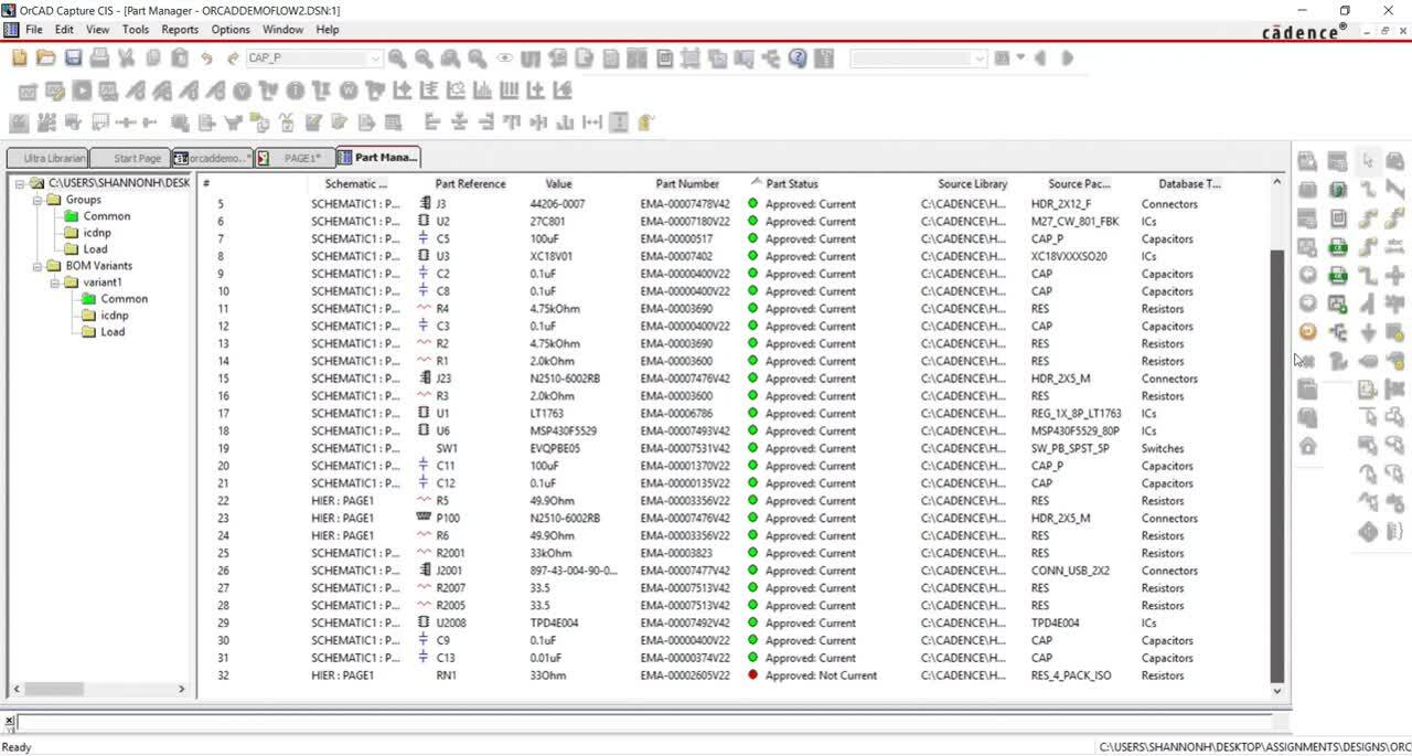
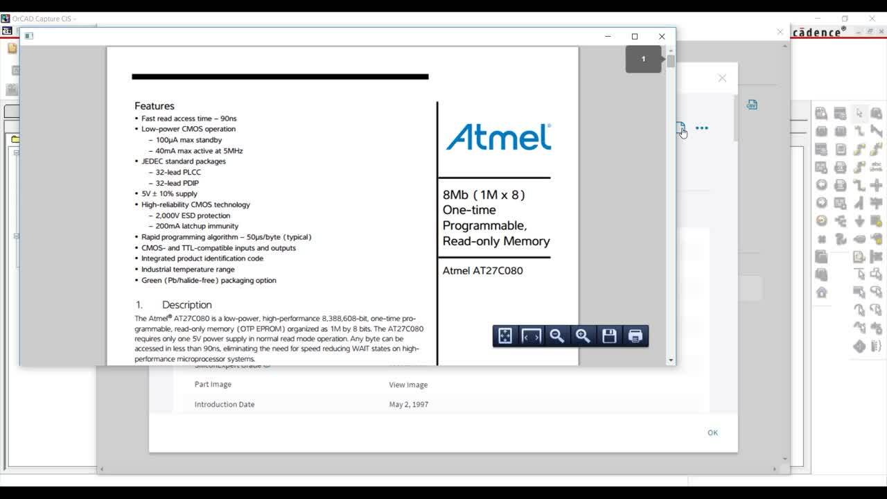
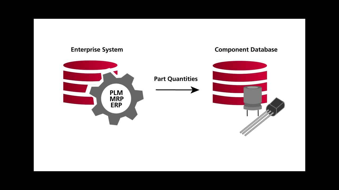
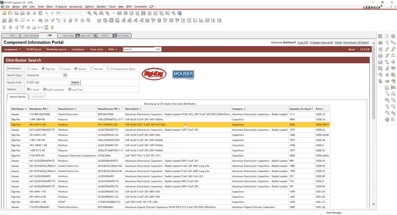
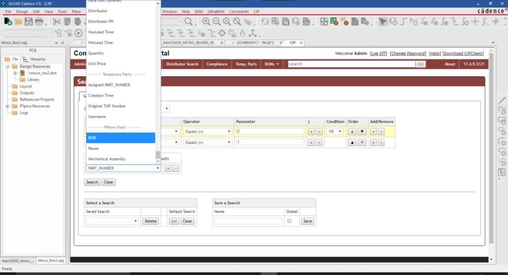
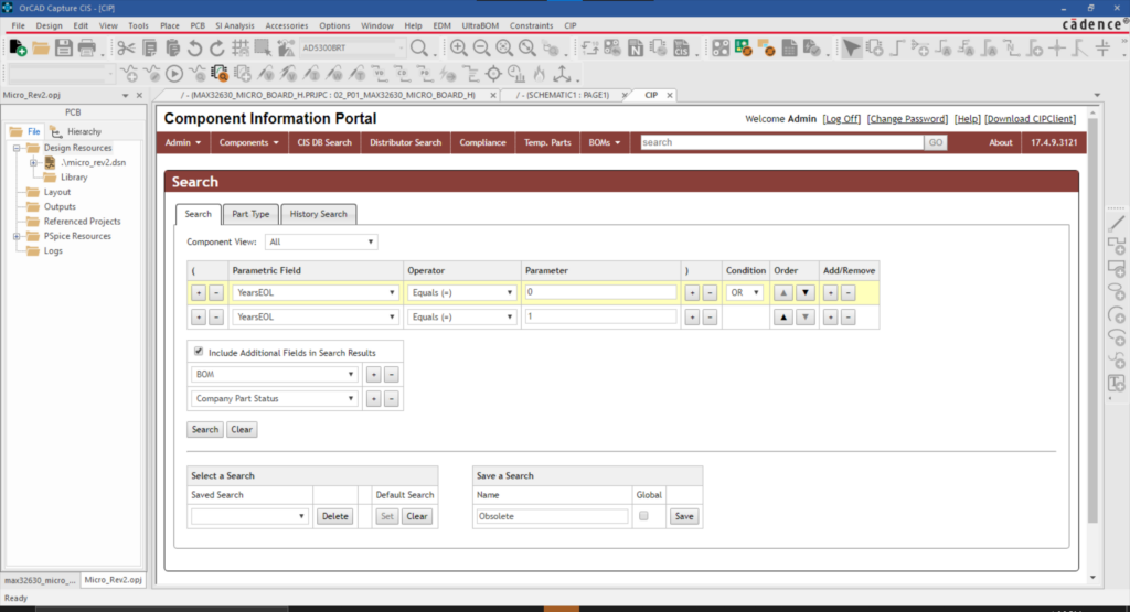
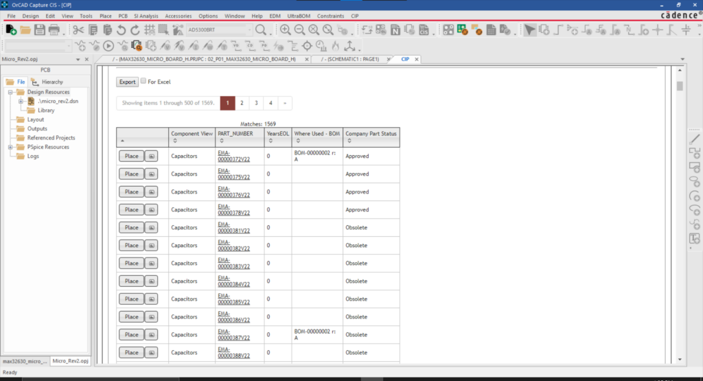
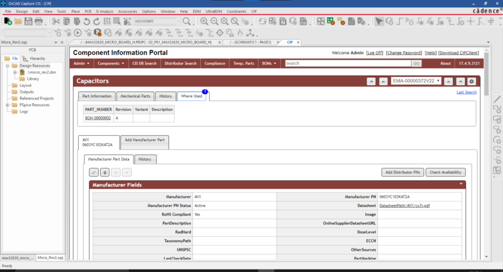
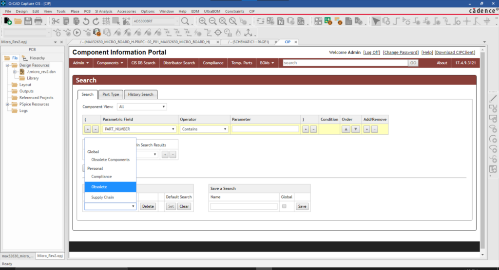
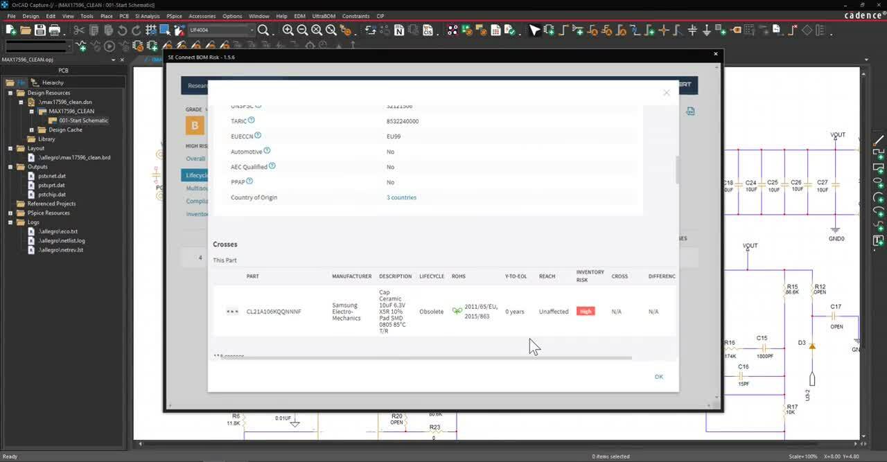
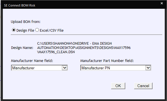
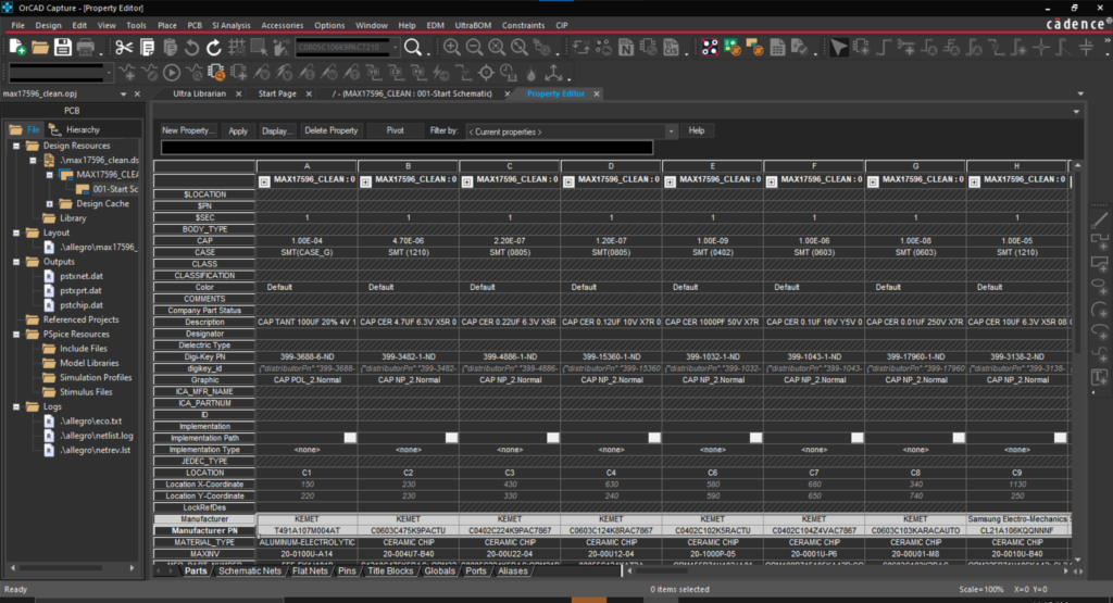
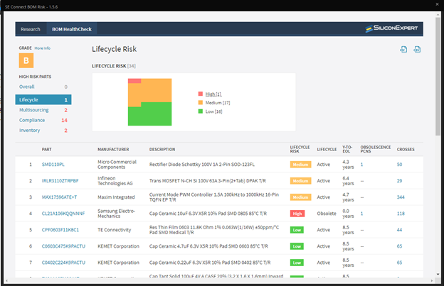
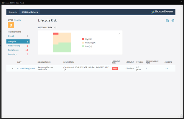
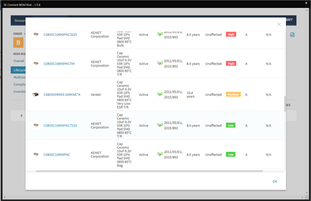
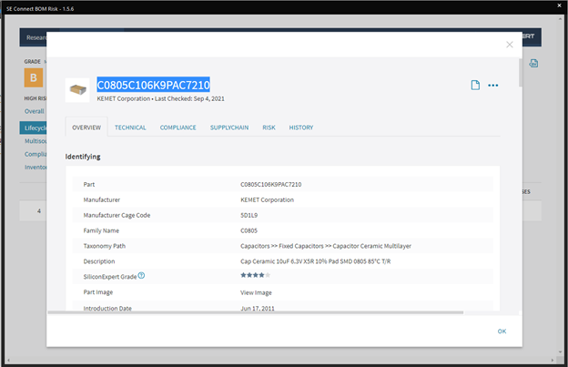
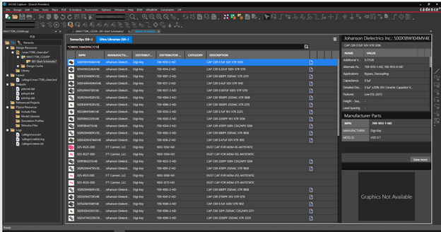
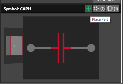
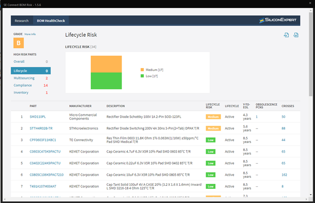
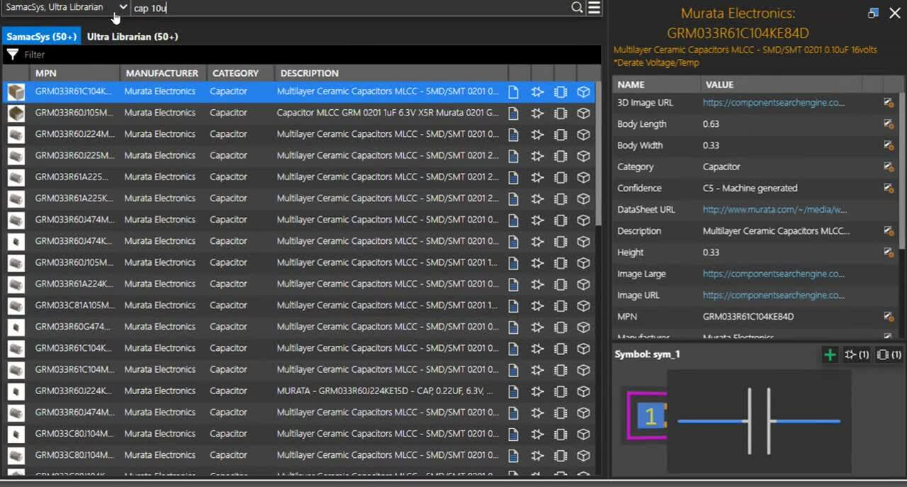
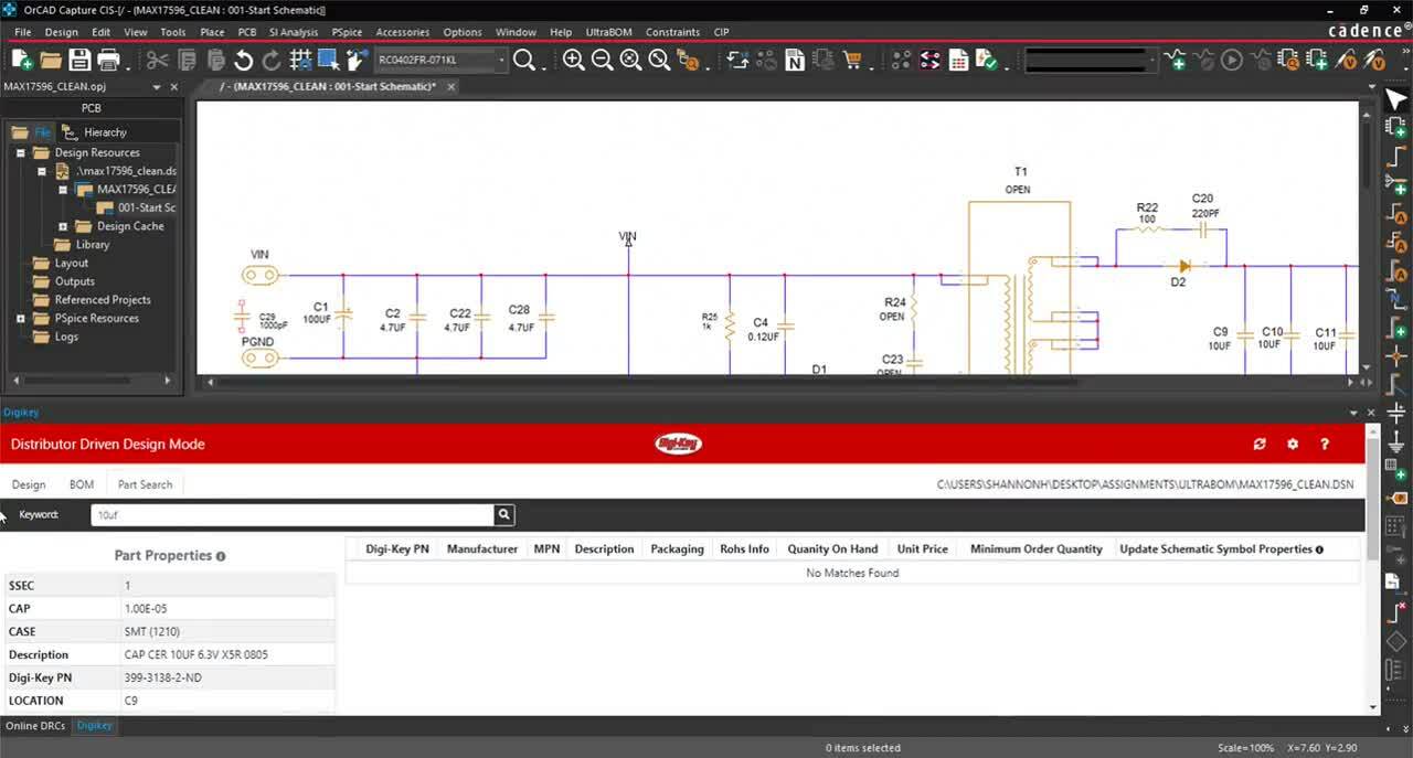
  • ★ Supply Chain Integration
    Having a component library that includes or incorporates real-time data about availability, turnaround times, and even component life-cycle status can make your part procurement process much more efficient. Having to make component changes downstream can greatly increase development time and costs.

  • ★ Simulate and Analyze Signal Flows
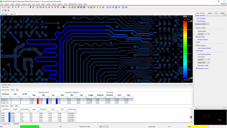
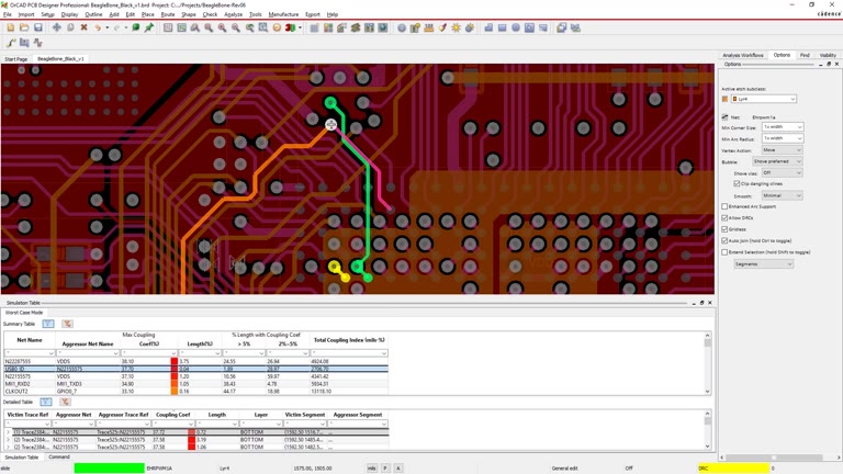
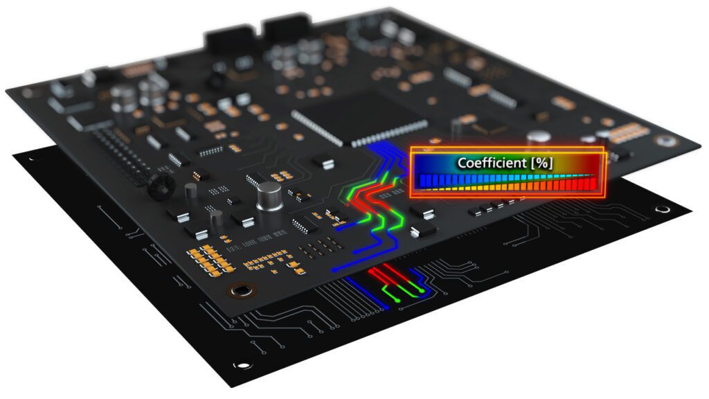
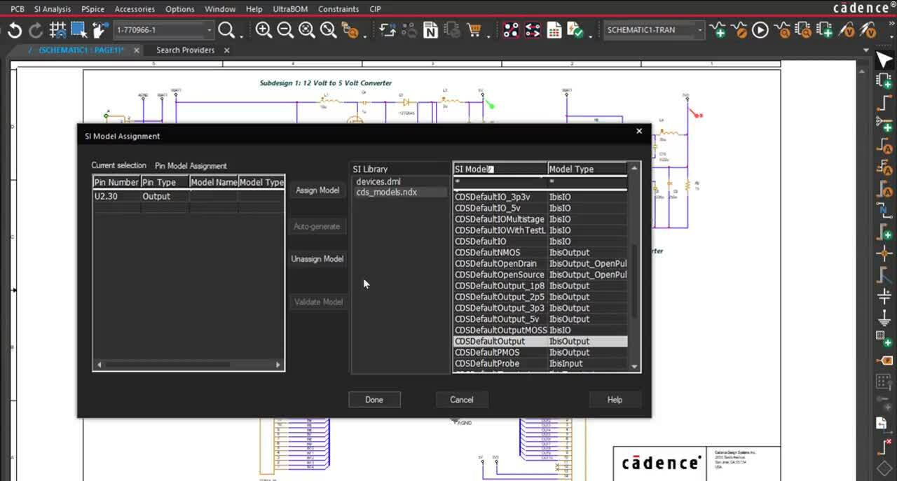
    Simulating your circuit’s operation and testing RF and microwave signal flow before the functional testing stage can substantially reduce development time and lower costs for engineering resources and excessive, unnecessary board spins.

  • ★ Simulate and Analyze Power Distribution
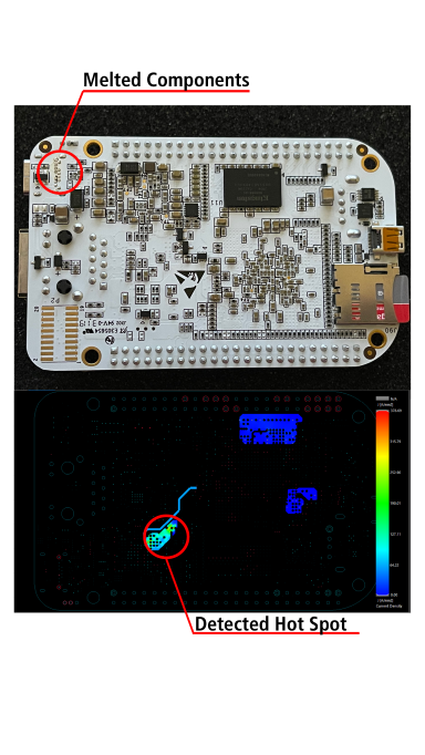
    Adequate power distribution is a major concern for many designs. Failure to meet power requirements for your board components, especially ICs, can result in erroneous results. The capability to simulate operation during design ensures your board’s PDN will satisfy on-board and intra-board objectives, saving you from potential board failures and recalls that can be quite expensive.

  • ★ Simulate and Analyze Thermal Distribution/Dissipation
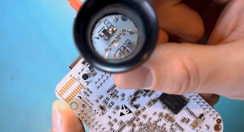
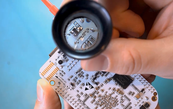
    For high-power components or elements, such as processors and power supplies, the ability to dissipate heat quickly is a mandate that, if unmet, leads to part and board damage. Therefore, this capability can potentially save high unnecessary costs.

  • ★ More Efficient DFMA Analysis
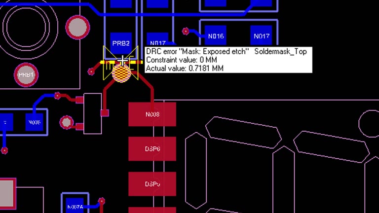
    For most PCBA design packages, DFM verification is a series of back and forth between DFM checks and manual corrections that wastes engineering resources. The alternative of not performing DFM and DFA verification can be increased design⇒build⇒test (DBT) cycles, which is also wasteful. Real-time integrated DFM solves this problem, improving your design process and lowering costs.

Implementing software design support tools that include one or more of the above capabilities will enable you to design faster and more efficiently, lower development costs, and improve your ROI.

EMA Design Automation is a leading provider of the resources that engineers rely on to accelerate innovation. We provide solutions that include PCB design and analysis packages, custom integration software, and engineering expertise, which enable you to create more efficiently. For more information on how to best manage electronic product design cost and ROI and how we can help you or your team innovate faster, contact us.

How to Quickly Determine where Obsolete Components are Used

A centralized component database provides access to verified and approved parts for your entire team; however, when components become obsolete it can be impossible to remember where they were used. Identifying and replacing these obsolete components is vital when reusing intellectual property or creating a new revision of an existing design. With OrCAD Component Information Portal (CIP), you can quickly identify the obsolete components and determine where they were used in your designs with saved searches.

This how-to provides step-by-step instructions for creating a saved search in OrCAD CIP to determine which designs contain obsolete components.

How-To Video

Configuring Database Search

Step 1: Select CIP > Open CIP from the menu and enter your login information.

Note: The CIS DB Search tab is automatically opened in the CIP window.

Identifying Components that are End of Life

Step 2: Enter the desired search parameters. To identify components that have 0 years until “End of Life,” configure the following parameters:

  • Parametric Field: YearsEOL
  • Operator: Equals (=)
  • Parameter: 0

Note: The YearsEOL parameter is available for users that have purchased the CIP Compliance Module and estimates the number of years until a component becomes obsolete. Saved searches are fully customizable and can search numerous component parameters including Company Part Status, Values, Manufacturing information, and more.

Step 3: Select the + under Add/Remove.

Note: This has automatically added a Condition to the search parameter.

Adding a Parameter to the Component Database Search

Step 4: Set the condition to OR.

Identifying Components that are near the End of Life

Step 5: Enter another search parameter. To identify components that have 1 year until “End of Life,” configure the following parameters:

  • Parametric Field: YearsEOL
  • Operator: Equals (=)
  • Parameter: 1

Including Additional Fields

Step 6: Select Include Additional Fields in Search Results.

Note: This displays additional parameters within the search results, allowing you to review all relevant information without selecting each individual component.

Identifying the BOM Where a Component is Used

Step 7: From the drop-down selection, choose BOM under the Where Used section.

Note: This will automatically identify the Bill of Materials (if any) where the component is used.

Step 8: Select the + next to the BOM parameter.

Step 9: From the drop-down selection, choose Company Part Status.

Reusing a Component Database Search

Saving Parameters to Reuse a Component Database Search

Step 10: Under Save a Search, enter a name for the search.

Note: Selecting Global will make the search available for all users. If global is not selected, the search will be available locally.

Step 11: Select Save and close the Search Saved Successfully window.

Searching for Part Obsolescence

Step 12: Select Search.

Searching Database for Obsolete Components

Step 13: View the search results to identify components that are 0-1 years away from obsolescence and determine where these components are used.

Identifying BOMs Associated with Obsolete Components

Note: Selecting a part number will bring you to the component page in the database. Here you can view additional component information as well as the corresponding BOM.

Reusing Saved Search Parameters

Step 14: Return to the CIS DB Search tab. The newly saved search is available in the drop-down selection under Select a Search and can be used to expedite future searches.

Wrap Up & Next Steps

Easily find desired components in your centralized database with the ability to save custom searches locally or globally in OrCAD CIP. This method helps identify obsolete components and where they are used, allowing you to replace components as needed for future design revisions. For more information and in-depth training on additional features, view our E-Learning and instructor led courses for OrCAD Capture CIS and CIP.

How to Identify Obsolete Parts and Find Viable Alternatives

Component availability and lifecycle aren’t static. With supply chain issues on the rise this can create many issues during the design process, regardless of the length of your design cycle. Whether you are completing a new design or updating an existing one, it’s likely at least one component can no longer be purchased due to low inventory or part obsolescence. To keep your design on track, it is important to identify obsolete parts and potential issues early in the design process. With SE Connect BOM Risk App, vital supply chain information is integrated directly into the schematic environment, making it easy to analyze, research, and guarantee successful component sourcing.

This how-to will help you automatically identify obsolete parts and high-risk components in the design, find viable alternatives, and replace the component within OrCAD Capture using the SE Connect BOM Risk App.  

How-To Video

Integrating Supply Chain Information

Step 1: Select Accessories > Silicon Expert > SE Connect BOM Risk from the menu.

Mapping Manufacturing Information for SE Connect BOM Risk App

Step 2: Map the Manufacturer Name field to the appropriate property in the schematic property. Map the Manufacturer Part Number field to the appropriate schematic property. Click OK.

Note: If you do not know these fields within your schematic, right click on the schematic page in the project hierarchy and select Edit Object Properties.

Identify the correct property for Manufacturer and Manufacturer Part Number.

Step 3: Enter your email address and password and select Login.

Note: The design will be analyzed, and a summary of the part statistics will be shown on the screen.

Step 4: Click Continue.

Identifying Supply Chain Risk

Identifying Risk of Component Obsolescence

Step 5: Select Lifecycle from the Risk Categories.

Note: Here you can view lifecycle information for all the components in the design including lifecycle status, years-to-end-of-life, obsolescence product change notices, and available crosses.

Identifying High-Risk Components in OrCAD

Step 6: Select the High lifecycle risk from the chart and select the obsolete component.

Note: This filters the components to show only those with a high lifecycle risk.

Addressing Supply Chain Concerns

Step 7: View the available crosses.

Note: A cross is an alternative component. Additional information can be viewed when determining a viable cross including the manufacturer, description, lifecycle status, ROHS compliance, years-to-end-of-life, REACH compliance, inventory risk, cross grade, and differences between the original component and the cross.

Identifying Possible Alternate Components

Step 8: Select C0805C106K9PAC7210 from the list of available crosses to view additional information.

Selecting a Replacement for Obsolete Components

Step 9: Use CTRL-C to copy the part number. Close the SE Connect BOM Risk App.

Step 10:  In the schematic, delete the high-risk, obsolete components.

Step 11: Select Place > Search Providers from the menu and login with your credentials.

Finding Component Models for Alternate Components in OrCAD

Step 12: Select the Ultra Librarian tab. Paste (CTRL-V) the new part number in the search field and Search.           

Step 13: Select Place Part.

Replacing Obsolete Components in OrCAD

Step 14: Click to place the component in the design.

Note: For SE Connect BOM Risk to incorporate the new component information, the appropriate manufacturer and manufacturer part number fields must be completed correctly. Verify this by selecting the schematic in the project hierarchy. Right click and select Edit Object Properties. Find the newly added components and ensure the correct fields are completed. Copy and paste the manufacturer and manufacturer part number as required.

Improving Design Longevity

Step 15: Select Accessories > Silicon Expert > SE Connect BOM Risk from the menu.

Step 16: Click OK to confirm the Manufacturer and Manufacturer Part Number mapping. Click Continue.

Reducing Component Risk with SE Connect BOM Risk App

Step 17: Select Lifecycle from the risk categories to view the updated lifecycle risk.

Note: The high-risk, obsolete components have been replaced in the design and SE Connect BOM Risk has been updated accordingly, in real-time.

Wrap Up & Next Steps

SE Connect BOM Risk App helps you analyze the inventory, lifecycle, multi-sourcing, and compliance risk for components in your design, identify obsolete parts, and select alternative components to resolve component issues early in the design process. With this knowledge, components can be replaced in the schematic before moving to PCB layout, reducing the likelihood of design re-spins and delays during assembly. Incorporate live supply chain information directly within your schematic to ensure ideal component selection with OrCAD and Silicon Expert. Get started with the SE Connect BOM Risk App to quickly identify supply chain issues with a free trial and learn more about how to effectively manage PCB design data with our e-book.

How to Ensure Approved Parts are Selected for Designs

For a PCB to be assembled within the project timeline, components need to be sourced quickly. Often a centralized database of approved parts is created to assist in component selection; however, with multiple engineers working on a project, guaranteeing only approved parts are used in the design is nearly impossible. With OrCAD Component Information Portal (CIP) you can easily implement safeguards through user roles, permissions, and customization and hide obsolete components from view.

This how-to will provide step-by-step instructions on how to utilize the Hide Feature in OrCAD CIP to guarantee only approved parts are shown for specific users.

How-To Video

Opening OrCAD CIP

Step 1: Open a design in OrCAD Capture CIS 17.4.

Opening OrCAD CIP from the Schematic

Step 2: Select CIP > Open CIP from the menu.

Step 3: Log in with username and password.

Editing Component Database Permissions

Accessing Administrator Features in OrCAD CIP

Step 4: Select Admin > Users, Roles & Permissions from the CIP menu.

Note: User roles, permissions, and configurations are only available to Administrators. 

Hide Rule in OrCAD CIP

Step 5: Select the Hide Rule tab.

Hiding Obsolete Parts in the Database

Editing the Hide Rule Settings in OrCAD CIP

Step 6: Click the Edit button in the leftmost column.

Enabling the Hide Rule in OrCAD CIP

Step 7: Check Enable.

Step 8: Select Company Part Status from the drop-down selection under Hide Part Field.

Step 9: Add Obsolete as the Values and click the plus sign.

Step 10: Select Read Only from the drop-down selection under Apply to Roles and click the plus sign.

Step 11: If desired, add a comment for the rule.

Hiding Obsolete Components from Users

Step 12: Click the checkmark to save the rule.

Note: Obsolete parts will no longer be displayed for users with Read Only access, ensuring only approved and available components will be selected for new designs.  

Wrap up & Next Steps

Hide obsolete parts from view in your centralized component database and guarantee selected components are up-to-date and approved with customizable roles, permissions, and configurations in OrCAD CIP. For more information and in-depth training on additional features, view our E-Learning and instructor led courses for OrCAD Capture CIS and CIP.

OrCAD Capture Essentials

Schematic Design with

OrCAD Capture Training Courses

OrCAD Capture Essentials

Learn all the necessary steps required to create a schematic using OrCAD Capture. New users will learn the essentials needed to generate a design, how to navigate the tool, run DRC checks, prep the design for netlisting, and generate BOMs.

Includes an OrCAD Certification Opportunity.

There are no prerequisites for this course.

What you will learn:

  • How to build new parts and symbols
  • Design-checking best practices
  • Techniques for assigning reference designators
  • Creating a BOM (Bill of Materials)
  • Adding part and net properties
  • Creating flat designs

OrCAD Certification Included*

OrCAD Schematic and PCB Front-to-Back Flow

This class is a comprehensive course aimed at helping students learn an efficient, front-to-back schematic and simulation workflow. This package includes Capture Essentials and PCB Editor Essentials training.

Includes an OrCAD Certification Opportunity.

There are no prerequisites for this course.

  • How to build new parts and symbols
  • Design-checking best practices
  • Techniques for assigning reference designators
  • Creating a BOM (Bill of Materials)
  • Adding part and net properties
  • Creating flat designs
  • Construct design libraries
  • Import logic design data
  • Define design rules
  • Interactive placement features
  • Pin Swapping
  • Route interactively
  • Run automatic glossing
  • Create copper areas
  • Generate manufacturing output and documentation

OrCAD Component Data Management with CIS and CIP

This one-day class will cover component data management with Cadence OrCAD Capture CIS and the OrCAD Component Information Portal™ (CIP), including product interface fundamentals, automating the part introduction process, and effectively managing the part database.

It is recommended that students have a pre-requisite knowledge and proficiency in OrCAD Capture Schematic editing.

What you will learn:

  • Manage parts and symbols in a relational database
  • Assign user privileges
  • Track historical changes of active and legacy parts
  • Manage the integrity of active and historical parts
  • Use distributor searching to locate necessary parts
  • Align new part introduction with corporate protocols
  • Create and formalize new parts
  • Link legacy data to approved parts
  • Swap out parts using Link Database Part
  • Finalize and document the design
  • Manage variants

Register for a Class

Why OrCAD

OrCAD PCB Design

Solve Your Toughest PCB Design Challenges with OrCAD

You need a dependable PCB design tool that can scale with your growing business. See why PCB design teams across the world depend on OrCAD to create high quality, reliable products. 

Over 50,000 Engineers & Counting

Instant Design Feedback While You Work

Your CAD tool should provide you with feedback when you need it, as you design, so you can make intelligent design decisions up front.  Get out of the Design – Check – Fix – Repeat cycle with the real-time design features only available in Cadence. With real-time design feedback, identify issues as they happen so you can address them when they are easiest to solve.

See Real-Time Design in Action >

Architected to Scale With You

The pace of change in electronics can be intense. You need a solution designed to keep up and grow with your needs. Stay ahead of the competition, technology changes, and innovate faster with the industry’s only fully-scalable design platform.

Explore OrCAD Design Suites >

Get Your Design Right the First Time

Getting boards back from manufacturing can be a nerve-racking experience, but it does not have to be. With the advanced DFM rule checking, real-time feedback, and analysis capabilities in OrCAD you can be confident your design will be up and running the first time.

Complete PCB Design Innovation Platform

OrCAD is built to support you from concept to production and beyond. With OrCAD, address all your design challenges in a single, unified environment.  Seamlessly get your design done on-time, the first-time by leveraging tools built to help you design for peak productivity, accuracy, and speed. Experience the future of PCB design with OrCAD.

CREATE

Industry Standard Schematic Capture

Design entry is powered by the world’s most used schematic capture solution, OrCAD Capture. Used on countless designs across all industries and levels of complexity, OrCAD Capture provides the perfect mix of ease of use and functionality to support your design requirements.

KEY CAPABILITIES

Easy & Intuitive

Quickly create clear and concise multi-page, hierarchical schematics with ease. Compare versions, generate bill of materials (BOM), and create pdf documentation at the touch of a button.

Integrated

Always know what changed with seamless sync of data between logical and physical. Integrated simulation engines let you perform analysis inside your schematic design environment, preventing rework and data loss.

Correct By Construction

Say goodbye to late-stage design changes with instant design feedback. Easily define and validate your design intent with real-time design rules checks, constraint definition, and pre-layout SI analysis. Then, seamlessly pass this data along to implementation—setting you up for design success right from the start.

Libraries Included

Be productive immediately with access to millions of popular CAD symbols footprints, and 3D models directly within the software. Libraries are the last thing you want to worry about and with OrCAD, you no longer have to.
DESIGN

Route with Precision and Accuracy

Over half of design cycle time can be spent in placement and routing. Complete even your most complex design with accuracy and speed with the industry’s leading PCB implementation solution and see how PCB design is meant to be.

KEY CAPABILITIES

Powerful Route Engine

Built on the Allegro PCB Editor architecture equals an unmatched placement and routing experience. 64-bit performance, real-time updates and feedback, intuitive interactive and automated routing, as well as comprehensive rules and route guidance support give you the tools needed to complete your designs fast and with confidence.

Instant Design Feedback

Don’t wait until the end of the project to find all the issues you need to fix and change. Get instant feedback as you design with on-canvas guidance and notifications, so you can solve issues before they have a chance to become an ECO.

Integrated 3D Engine

View, manipulate, and evaluate your design in 3D right from within the PCB design platform. Identify collisions, see how your design performs during flex bends, and view the effects of mechanical elements such as heat sinks and enclosures in realistic 3D. Quickly adjust and see changes update instantly.

Scalable & Extensible

As your needs grow, so can your design tool. Our unique, scalable architecture allows you to seamlessly add capabilities like advanced routing and team design as needed, all leveraging the same data model eliminating any needs for translation.
ANALYZE

Comprehensive Simulation and Analysis

Know your design is ready for production with our complete set of analysis and simulation options. Run thousands of design scenarios, identify, and fix issues before the first physical prototype is ever produced.

KEY CAPABILITIES

In-design Analysis

Analyze your data where it is. Cadence analysis is deeply connected to the PCB design platform to provide quick and accurate analysis so you can easily take action. No clunky translation or time spent pushing data between tools.

Actionable Insights

Easily visualize and identify the impact of your analysis results. From improving yield and identifying parts likely to fail to displaying results of multi-gigabit simulations, you will have the guidance you need to make the right decision based on your simulations.

Optimize and Verify

Analyze your design at all stages of the process. Identify optimizations and test design alternatives early where the cost of change is lowest. Then take advantage of our unmatched accuracy and capacity to perform final sign-off and verification, all in one platform.

SI, PI, Thermal, and SPICE

Leverage a full suite of analysis engines and explore all aspects of your design from analog mixed-signal, signal integrity, power integrity, and even thermal affects. Mix and match engines easily to meet your design requirements and move to production with confidence.
BUILD

Go to Manufacture with Confidence

Sending your design to production can be a tense experience. Many have come to expect manufacturing changes and issues to happen, slowing the design cycle and often leading to long nights and weekends for the engineering team. It doesn’t have to be that way. Go to manufacturing with confidence knowing you have been checking for manufacturing issues along the way with our real-time DFM checking and rules support.

KEY CAPABILITIES

Instant DFx Feedback

If you can’t build it, you can’t release it. Leverage real-time DFx (manufacturing, test, fabrication, and assembly) checks as you design and get instant feedback if a potential manufacturing issue will occur.

Automated Manufacturing Outputs

Generating the correct files and providing accurate and clear documentation is critical for design success. With OrCAD, ensure a smooth manufacturing process without manual effort by automatically generating your design documentation and manufacturing output files.

Effortless MCAD Integration

Ensure fit and function by seamlessly synchronizing your design with mechanical before you build. Easily communicate and track changes between ECAD and MCAD so everyone is on the same page and your project is on track for success.

DesignTrue DFM

Collaboration with your manufacturing partner early and often is key to success. Bring this collaboration into your design with the DesignTrue DFM partner program. Easily bring your manufacturing partners’ design rules into your design and build a true, correct-by-construction flow by checking your design against your intended manufacturing line as you go.
MANAGE

Your Data Where You Need it, When You Need It

Keeping track of design revisions, managing part availability and compliance, and updating your PLM can seem like another job. OrCAD provides automated capabilities to handle these necessary tasks quickly and efficiently without having to leave your CAD environment. 

KEY CAPABILITIES

Automated Revision Control

Get rid of the needless email chains and finger pointing to try and figure out who changed what when. Easily manage design revisions with automated check-in, check out, easy roll-back, and complete design version history at your fingertips.

Seamless Team Design

When working in a team, ensuring everyone is on the same page is critical. Effectively collaborate with quick and easy definition of project responsibilities and access, and seamless communication among multiple team members.

Component Sourcing and Library Management

Reduce errors and remove redundancy through the deploy of a shared library that can be accessed by your engineering team. Augment component library data with part pricing, availability and lead times, and automatically update your projects as data changes. Make your part library a competitive advantage not a design challenge.

Enterprise Integration

Your design is often part of a whole and as such, will need to be managed in a company PLM system or similar. Easily synchronize your design data with PLM and surface contextual data from PLM such as corporate-approved part numbers directly in your CAD tool and ensure a smooth transition to production.
Learn More

Products

Explore the full breadth of OrCAD technologies. Designed to scale with your needs, you can easily select the technologies required to solve your unique design challenges while maintaining a common, flexible design environment that can grow as you do.

OrCAD PCB Designer Suite

Powerful, comprehensive PCB design packages

Complete PCB Design Solutions Including:

Schematic | Layout | Routing | Manufacturing | Analysis

Starting at $1,300 / year

OrCAD PSpice Designer Suite

Advanced virtual prototyping solutions for first pass PCB success

Complete Analog / Mixed Signal Analysis Including:

Schematic | SPICE simulation | Reliability Analysis | Electro-Mechanical Sim 

Starting at $2,400 / year

Compare PCB Design Suites

Schematic Entry and Libraries
OrCAD Capture Schematic Entry
Hierarchical and Multi-Sheet Schematics
Snap Functions and Grids
Block Diagram Support
Schematic Symbol Editor
Starter Library with Integrated Cloud Library of Millions of Symbols, Footprints and 3D Models and Custom Library Creation
Comprehensive Project Hierarchy
Rule Definition and Management with Real-Time Design Rule Checking
Open Design Framework
Integrated Spice and SI Simulation
Automated Design Cache
Customizable Component Properties and Bill of Material (BOM) Creation
Graphical Design Compare
Automated Annotation/Back Annotation and Ref Des Assignment
Intelligent PDF Output of Schematic
Built-in Translators (Altium, Mentor, Eagle, more)
PCB Layout Creation and Automatic Netlist Generation within your Schematic
Component Data Management
Integrated Access and Component Placement from a Centralized Component Database
Integrated Part Manager
Part Status Notification
Design Variant Support and Color-Coded Variant Display
Parametric Part Search
Temporary Part Management
Symbol and Footprint Preview
Automated Zero-Touch Bill of Material (BOM) Creation
BOM Templates
Relational BOM Support
BOM Variant Support and Variant Reporting
Cloud Enabled Services
Cloud-Based Workspaces
Customizable Permissions
File Management and Version Control
Integrated Part Authoring and Management
Promoted Library of Symbols and Footprints
Automatic Population of Parametric Information
Association of Simulation Models, Symbols, Footprints, and Datasheets
Managed User Roles
LiveBOM: Real-Time Supply Chain Analysis
Advanced PCB Layout and Routing
Real-Time Design Synchronization
Cross Probing and Cross Placement of Components Between Schematic and PCB
Automated Intelligent Component Placement Using Quick Place
Component Footprint and Padstack Wizard and Editor
SKILL (programming language, runtime, macro and scripting support)
Cross Section Support and Editor with Unlimited Layers
Splitplane Support
Dynamic Shapes and Pad Suppression with Real-Time Plowing and Healing
Extended Net (XNET) Creation and Rules
Differential Pair Support
Automatically Route Nets by Pick
Interactive and Advanced Routing
Stacked Via Edit and Move
Blind and Buried Via Support
Intelligent PDF Output from Board Design
Import/Export of Cross Section, Colors, Design Rules and Parameters
Design Review and Markup
Autorouting
Interactive Delay Tuning
Dynamic Heads-up Display for Critical Nets
Group Route Via Pattern and Via Array/Shielding
Segment Over Void Detection
Placement Replication
Symphony: PCB Co-Design
Rule-Based Design
Constraint Manager
Physical and Spacing Rules
Via-in-Pad and Pad Entry/Exit rules
Differential Pair Rules
DFx Rules and Checks
Real-time Active Design Rule Checks (DRC)
Constraint Manager Analysis Mode
Electrical Rules
Layer Set and Matched Group Rules
Propagation Delay Rules
Pin Delay Inclusion and Z-Axis Delay Support
Region-Based Rules
Return Path Rules
3D Clearance Rules
Automated Rigid Flex Design
Region-Based Rules
Inter-Layer Checks
Hug Contour Routing
Multi-Cross Section and Zone Table Chart Support
Dynamic Zones with Cross Hatch and Solid Planes
3D ECAD/MCAD Co-Design
3D Visualization with Collision Detection
Interactive 2D/3D Cross Probing and Cross Placement
3D Bending (FLEX)
MCAD/ECAD Incremental Design Data Exchange (EDMD)
Mechanical CAD Interface
Bi-Directional OrCAD and SOLIDWORKS integration (MCADX)
3D Clearance Checking and Design Rule Violations
In-Design Simulation and Analysis
Transient, DC, AC, Bias Point PSpice Analysis
PSpice Modeling Applications
Digital and Basic Analog Device Libraries
Waveform Analysis
IBIS Model Support
Pre-Layout Signal Integrity Analysis
Post-Layout Signal Integrity Analysis
Real-Time Impedance and Coupling Analysis
Placement Density Analysis
Real-Time Electrically Aware Placement Vision to Optimize PCB Layout
Real-Time Visual Routing Trace Optimization and Identification of Common Traces Issues
Manufacturing, Assembly, and Testing Support
Output Formats: Gerber 274x, NC Drill, NC Route, IPC-2581, ODB++, IPC-D-356 Netlist
PCB DesignTrue DFM Wizard and DFM Partner Portal Access
Embed Assembly Notes and IPC-2581 Specs Within PCB
2D Drafting and Dimensioning
Automatic Silkscreen Generation
Variant Assembly Drawing
One-Click Release to Manufacturing Export
LiveDoc: Real-Time Manufacturing Documentation
PCB Panelization
Dynamic Shaped-Based Fillet Support and Line Fattening
Backdrilling
DFT: Automatic Test Prep, Test Point Rules
Capture_CIS

OrCAD Capture

One of the most powerful design environments for taking today’s product creation from concept to production. Quickly, easily, and intuitively create complex schematic designs with hierarchical, reuse, and variant design capabilities.

Buy | Free Trial | Learn More

Constraint Designer EE

Make your design requirements an inherent part of the design process. A unique, wizard-based approach quickly defines requirements for your critical nets (such as DDR) and drive this data into PCB implementation for accurate and fast PCB layout and routing.

Buy | Learn More

OrCAD Capture Cloud

Access OrCAD Capture wherever you are with OrCAD Capture cloud. View, design, and evaluate schematics all within your browser.

Free Access | Learn More

PCB Editor Pro

OrCAD PCB Editor

OrCAD PCB Editor provides a concept to production design environment. Achieve design success with powerful PCB Design capabilities, scalable design environments and proven technology.

Buy | Learn More

OrCAD Documentation Editor

Quickly create the necessary manufacturing drawings to drive PCB Fabrication and Assembly with OrCAD Documentation Editor. With intelligent automation, complex PCB documentation is created accurately in a fraction of the time, ensuring manufacturing success.

Learn More

OrCAD DFM Checker

Easily identify issues in your design created during the manufacturing process with OrCAD DFM Checker. Perform a comprehensive manufacturing analysis while you design and address potential issues before fabrication to avoid time-to-market delays and costly re-designs.

Learn More

PCB Clustering for OrCAD

PCB Clustering for OrCAD provides AutoClustering technology, intelligent design (IP) reuse, and replication technology that can significantly reduce board placement time.

Buy | Learn More

Productivity Toolbox

OrCAD Productivity Toolbox provides a comprehensive suite of utilities designed to increase efficiency throughout the PCB design. With the enhancement and optimization of existing PCB layout capabilities, you can save time on monotonous tasks and focus on design.

Learn More

Pspice Advance analysis

PSpice

Optimize your designs and improve reliability, predictability, yield, and cost with an industry-leading, complete circuit simulation and verification solution.

Buy | Learn More

Sigrity Aurora

Detect and correct signal and power integrity issues throughout your PCB design with the integrated technology of Sigrity Aurora. Sigirty Aurora users can perform pre-layout analysis using “what-if” scenarios to develop accurate design constraints and confirm circuit functionality with in-design and post-layout analysis ultimately reducing design iterations.

Learn More

Sigrity

Easily screen a PCB design for signal quality without having to be a signal integrity expert. With Sigrity go beyond the simple geometry-based DRC and evaluate the entire design for impedance discontinuities, excessive crosstalk, return path discontinuities and more.

Learn More

AWR

Develop physically-realizable electronics ready for manufacturing and ensure success of your RF/Microwave designs with AWR. AWR allows you to model, simulate and verify all aspects of your design, including complex integrated circuits, packaging and PCB’s.

Learn More

EDM_4 (1)

OrCAD Engineering Data Management

Control your design data without ever leaving the OrCAD environment with revision control for schematic, PCB, and components. With OrCAD Engineering Data Management you can communicate, track changes, and ensure accurate and efficient team collaboration.

Learn More

OrCAD Component Information Portal

Part creation, verification and management is made easy with OrCAD CIP. Streamline your design process with a centralized part database to ensure the correct symbols and footprints are used by the entire team.

Learn More

SE CONNECT BOM Risk

Optimize part selection and ensure design success by analyzing components for availability, compliance, and reliability during schematic creation within OrCAD.

Buy | Learn More

UltraBOM

Frustration-free part purchasing and BOM creation with live distributor information directly within OrCAD.

Free Download | Learn More

Enterprise Connect

Seamless integration between your PCB Design environment and your PLM, MRP or ERP systems ensures design success by incorporating product lifecycles and inventory into your design decisions.

Learn More

How to Buy

Buy OrCAD

Get started with the only PCB Solution built to grow with you. 

For Students

Students have access to a full OrCAD academic license. 

Posted on

A Little Simulation Goes a Long Way – Preventing PCB Respins & Supply Chain Issues

It’s simple to know when a board is not functioning properly. The hard part is identifying the source of the problem; often leading to hours troubleshooting in the lab. This happened to me recently when analyzing an open-source design. An overheating problem was detected and clearly shown on the board by overheating, powering down, and melted components; however, the exact catalyst was unknown.


Using Sigrity Aurora, I was able to pin-point the problem area using current density analysis and adjust the design by slightly moving a single via to improve current flow and eliminate overheating (hint: the issue was not where the components were melting).


For DesignCon (12 weeks away at the time), we wanted to prove how this simple fix was able to resolve the hotspot by recreating the board with the correction. Should be easy right? We had the design files, the BOM, and the only change we made was to move a via and get a few new boards produced.
 

Enter the Supply Chain

Obsolete components due to the age of the board, coupled with current supply chain issues and chip shortages, made this impossible. As this was an open-source design and not my own, trying to source the required components became time-consuming and tedious; entering each component into a vendor website and trying to find comparable components to those that were unavailable.

With parts obsolete, extremely long lead times (up to 65 weeks), no stock, and backorders, producing an equivalent design in 12 weeks was not feasible. This had me thinking about how many designers are running into these kinds of issues and how they could have been prevented.

These supply chain and obsolescence issues could have been prevented had they been accounted for at the start of the design.

Prevent Respins – Prevent Supply Chain Challenges

One way to prevent supply chain issues when doing a respin is to prevent the respin in the first place. In the instance above a few minutes of simulation would have identified this issue and allowed the design team to fix it quickly before the boards were ever produced originally. This would have been ideal in my case but what if you need to make more of these boards in general? How could you ensure you won’t be giving your future self fits trying to deal with part sourcing issues?

How to Prevent Supply Chain Issues – It’s All About Data Access

These  supply chain issues have become more common in recent years causing companies to face difficulties when sourcing materials for their PCB designs and affecting time-to-market. These supply chain issues must be addressed throughout the design process to ensure timely component sourcing and keep design production on track. Proper planning and coordination between all involved parties will help to avoid these situations from arising in the first place. By having a clear understanding of the components (and their supply chain status) required to produce a product, designers can be made aware of potential delays. By keeping a close eye on inventory levels, obsolescence risks, and defining alternate sources, companies can ensure PCBs can be produced on schedule. While not everyone has the luxury of having a designated component engineer, there are tools that can aid in this process.

Supply Chain Insights On-Demand

If component obsolescence and the effects of the supply chain are analyzed and addressed during part selection, many of the issues I ran into could have been eliminated. Integrating supply chain information into your design process, helps engineers make informed component decisions and prevent any component sourcing, compliance, and obsolescence issues from the start.


SiliconExpert, is one service that provides direct access to vital supply chain information such as lead time, component availability and pricing, compliance information, and more. With a comprehensive risk assessment for all components in the design, high-risk components are automatically identified, and alternate components are provided to quickly find a comparable replacement. 

Incorporating Supply Chain Information Early is Critical to Design Success

While long lead times and part availability affect every PCB Design, component lifespan must also be considered. Components are bound to become obsolete at some point, but they can be managed to increase the longevity of your PCB Design. Even years later, many of these obsolete parts would not be an issue by incorporating supply chain information into the design process. For these high-risk components, the years-to-end of life would have been reported and alternate components with longer lifespans would have been selected.

In my case, I needed to reproduce a design with the same layout and components to show how moving one via could greatly affect design performance and reduce hotspots. While I could have quickly found similar alternatives for some of the obsolete or unavailable components such as resistors and capacitors, there is nothing I could do about lead times up to 65 weeks for vital ICs that could not be switched out. However, hindsight is 20/20.

Now that there are tools available to analyze the supply chain, it’s easier to keep design production on track and increase the longevity of your PCB. For now, we will have to wait until the supply chain stabilizes to produce the board I wanted to, but in the meantime, you can check out the original open-source board, thermal hotspot identification, and resolution in Sigrity at our 2022 DesignCon booth #1243.

PCB Design Data Management

DESIGN DATA MANAGEMENT SOLUTIONS FOR PCB DESIGN

Integrated Design Data Management, First-Pass Success

Avoid miscommunication, unnecessary respins, and manufacturing delays due to manual data tracking and storage. Take control of your design data today.

Transform Your Design Process with Well-Managed Data

LeverageIP

Leverage IP Effectively

Seamless library and file management allows you to easily manage your IP throughout your company.

Prevent Errors

Prevent Costly Errors

Verify the correct data is going into the design and send that data directly to manufacturing.

EliminateDelays

Eliminate Preventable Delays

Comprehensive compliance insights eliminate any late-stage surprises so you can be confident your design will be manufactured on time.

Collaborationweb

Increase Collaboration

Keep every stakeholder on the same page with revision control and cross-functional collaboration abilities.

Design Data Confidence, Not Confusion

According to Aberdeen, best-in-class designers have cut down wasted design time due to data integrity issues by almost half with solid data management processes and tools. Eliminate wasted time, empower your team, and inspire manufacturing confidence in your designs with easily managed and maintained design data in OrCAD.

File and Library Management

Easily manage symbol and footprint libraries, design data, and documentation to create data consistency for your entire team. Design validation and automatic packaging of your manufacturing data ensures the correct revision of your design can be produced the first time.

Learn More >

Component Data Management

Easily manage your centralized component database, create new parts directly from distributor insights with OrCAD’s comprehensive suite of design data management solutions.information and deliver zero-touch, ready-to-order BOMs with direct access to a common library of approved and available parts.

Learn More >

Team Collaboration & Co-Design

Eliminate communication mishaps and ensure your team is always on the same page with built-in revision control and change tracking in OrCAD EDM. Be sure data will never be lost or overwritten ever again with customized permissions based on role assignments.

Learn More >

Integrated Part Information

Easily keep your part data in-sync between the component database and your design. With real-time part information and color coded part status it’s easy to identify obsolete, temporary, and approved parts to make informed part decisions while you design.

Learn More >

Compliance and Supply Chain Aware

Easily analyze individual designs or your entire component library to source components for availability and reliability with real-time access to supply chain and component data directly in OrCAD.

For Teams >

For Individuals >

Product Lifecycle Management

Ensure data integrity and streamline your component purchasing with seamless access to your company’s engineering-centric data through a bi-directional link between your component database and your company’s PLM, MRP, or ERP system.

Learn More >

Cross-Functional Collaboration

Easily collaborate and simplify your review process with all project stakeholders, including non-engineering users, with data access via a web client and custom user preferences for read-only access.

Learn More >

Release to Manufacturing

Streamline the generation of manufacturing data and ensure board success with the automatic generation of all necessary documents for manufacturing, including:

  • IPC-2581
  • ODB++
  • Artwork
  • IPC356
  • Fabmaster
  • Testprep
  • NC Route
  • NC Drill
  • Pick and Place
  • And more.

Learn More >

See Integrated, Easy PCB Design Data Management for Yourself

Watch our short demo showing how design data management can become a helpful part of your design flow not another task you are forced to do.

Solutions to Suit Your Unique Needs

Component Information System

Complete Integrated Centralized Part Database

Component Information Portal

Component Creation, Verification, and Management

Engineering Data Management

Revision Control, File, and Library Management for Teams

Enterprise Connect

Seamless integration between Design environment and your PLM, MRP or ERP Systems

SE Connect BOM Risk

Real-time compliance, availability, and supply chain information for your design.

CIP Compliance Module

Real-time compliance, availability, and supply chain information for your entire component database.

REQUEST A DEMO

OrCAD Version History

OrCAD Version History

Leadership in PCB Design Demands Constant Innovation

Cadence OrCAD is a driving force in the PCB design industry. In order to help designers keep up with the constant pace of change Cadence has been accelerating the pace of innovation delivering a stream of updates and product enhancements to users. The release history below provides insight into industry-first capabilities made available to customers such as real-time design, DesignTrue DFM, constraint manager, in-design analysis, and more.

New Feature Highlights:

Full Release History:

Version Notes:

  • Cadence provides bi-weekly updates to its products to fix issues and defects as quickly as possible for customers
  • New functionality is also delivered through quarterly incremental releases (QIRs).
  • Customers are encouraged to stay on the latest update within a release as they will not only get access to any fixes but will also have access to new features (as described below) available through the QIR stream.

Version 23.1.1

Products Covered: OrCAD X Capture CIS | OrCAD X PCB Editor| OrCAD X Presto | PSpice

OrCAD X Capture CIS

23.1.1

  • ASME 2 level Revision Scheme Support. Automatic ASME 2 level alphanumeric revision scheme within cloud workspaces.

  • LiveBOM Cross-probe. Cross-probe between LiveBOM and the schematic to efficiently identify at-risk components in the design. OrCAD-X Pro

  • LiveBOM On Premise CIS Support. Connect to on premise CIS database within LiveBOM to analyze supply chain risk for CIS database components in your schematic designs. OrCAD-X Pro

  • LiveBOM Enhancements. Enhancements to LiveBOM and ease of use with the inclusion of supply chain lead time and customizable property columns. OrCAD-X Pro

OrCAD X PCB Editor and OrCAD X Presto

23.1.1

  • Design Review and Markup Improvements. Easily archive and remove embedded comments to share the design with external users and partners.

  • 3D Enhancements. 3DX canvas has been improved in both OrCAD X PCB Editor and OrCAD X Presto to include cutting planes, material colors, transparency control for all 3D objects, 3D DRC display options, and measuring in 3D.

OrCAD X Presto

23.1.1

  • Object Visibility Improvements. Incorporate stipple patterns for improved object visibility. User-defined views allow you to save views and recall the visibility display in OrCAD X Presto.

  • Footprint Enhancements. Updates to editing footprints including mass editing of pin locations through the search panel, pad preview in search, and DXF import for footprints.

  • Paste Special Improvements. Preserve the location of copied shapes for easy replication.

  • LiveDoc Enhancements. Dimension improvements including alternate units and user-controlled text, panning and zooming improvements, ISO and ASME page sizes, and definition of export PDF location.

PSpice

23.1.1

  • ISO Transient Sources. ISO Transient sources for automotive applications including ISO 7637-2 for electrical disturbances form conduction and coupling and ISO 16750-2 for environmental conditions and related testing.

  • Performance Improvements. Parallel simulation support for parametric sweep, temperature sweep, and Monte Carlo Analysis on desktop to improve performance.

  • Noise Contributors. Control noise contributors in noise analysis to produce an accurate simulation.

  • Audio Simulation Support. Use a .wav file as a simulation input or export a .wav file as an output to perform audio simulations.

  • Simulation Personas. Use and create PSpice simulation personas as a simplified way to globally apply simulator options.

Version 23.1

Products Covered: OrCAD X Capture CIS | OrCAD X PCB Editor| OrCAD X Presto | PSpice

OrCAD X Release. Innovative design platform focusing on providing a cohesive and comprehensive solution for all design requirements.

OrCAD X Capture CIS

23.1

  • Enhanced Help Documentation. Cadence Doc Assistant presents help content as individual easy-to-read topics and has improved the speed and relevance of search capabilities. New documentation has been provided for library and part management, part authoring, and more.OrCAD-X
  • Enhanced Component Explorer. Access all the library sources along with complete part details in a unified view. The intuitive user interface provides access to various libraries supplied by Cadence, PSpice libraries and models, and external providers.
  • Integration with Content Providers. A new content provider has been integrated into the unified CIS environment. In addition to Ultra Librarian and SamacSys, SnapEDA can now be accessed directly through the schematic.
  • Integrated Part Authoring. Create new components from scratch using available libraries or existing parts from content providers. An easy-to-use dialog box lets you easily configure a description, category, logical symbol, footprint information, PSpice models, and electrical specifications. Incorporate lifecycle status, manufacturing part numbers, and more.
  • Part Template Creation. Quickly create parts from templates containing verified symbols, footprints, models and properties and organize the parts in the workspace efficiently.
  • Teams and Workspace Support.  OrCAD X provides a new collaborative development environment to create shared workspaces containing work-in-progress components, projects, libraries, and design files. Create multiple workspaces for different projects and user needs. Share workspaces, define user access and roles to efficiently collaborate with team members.
  • Workspace Content Management. Cloud optional workspace allows you to access data from anywhere and sync data between the local disk and cloud to keep all team members up-to-date.
  • Seamless Integration to OrCAD X Presto. OrCAD X Presto is fully integrated into Capture CIS allowing you to perform design synchronizations from the schematic to PCB and vice versa. Cross-probing capabilities between the schematic and PCB help to efficiently complete the layout design.
  • LiveBOM. LiveBOM is a dynamic bill of materials (BOM) that is generated using up-to-date supply chain data with zero configuration. The rich UI provides live part status from cloud libraries including real-time component availability, price data, alternative parts, life cycle status, dynamic part information and more.OrCAD-X Pro

OrCAD X PCB Editor

23.1


  • Enhanced Documentation. Cadence Doc Assistant presents help content as individual easy-to-read topics and has improved the speed and relevance of search capabilities.
  • Design Review and Markup.  Facilitate a collaborative design review environment with the ability to markup and comment design feedback directly in the PCB canvas. Markups are stored in the design database, streamlining the design review process. 
  • Counterbore/Countersink. Define secondary drill definitions on either the primary or secondary side.
  • Microvia Slot. Expanded the capability of microvia drill support beyond circle and square-plated holes to include microvia slot. This allows rectangular or oval-plated slots while following standard microvia constraints in the design.
  • Drilled Hole Padstack Definitions. Drilled hole fields for circle and square holes as well as round slot fields for rectangle and oval shot holes have been added for accurate unit-controlled values of the drill hole size before plating and tolerances.
  • Multi-Drill. Pitch values for rows and columns can now be defined to calculate the spacing automatically for a multi-drill.
  • Freeze/Unfreeze Dynamic Shapes. When dynamic shapes need to remain constant to protect critically circuitry and maintain design intent, suspend or freeze dynamic voiding instead of converting to static shapes. Once frozen, new objects entering a shape will not void and will generate a DRC error.
  • Zone Adherence for Symbol Pins. Components placed in a zone with some of the pins protruding into another zone can cause buried or floating pins. Easily check to verify that all pin pads of a component exist on the same placement layer.
  • Nested Zone Support. Designate stackup differences in particular areas of your rigid-flex designs by defining one zone inside another for scenarios where one shape needs to be surrounded by another.
  • Updated Zone Boundary Editing. Zone modifications can now be performed without activating Shape Edit Application Mode.
  • Fill-In Materials. Define the fill-in material for multi-layer PCBs to account for the different dielectric constants that affect the electrical characteristics of conductors running across the dielectric​.
  • Updated Dimension Line Width. Define dimension parameters to apply a line width globally for all dimensions.
  • Z-Copy Enhancements. Define the net during Z-copy to copy etch shapes to other layers. Incorporate a subclass wildcard to copy the shape to multiple layers.
  • Place Replicate Enhancements. A new delete option will remove routing from the previous module for components that are part of another module.
  • Netlist Import Enhancements. Reuse device files and component definitions that are currently in the design when loading an updated netlist.
  • Net Short Report. New net short properties report is available to easily find all the objects in the design with the Net short property to verify the nets being shorted.


OrCAD X Presto

23.1

  • OrCAD X Presto Release. A New layout environment offering a cutting-edge solution for PCB design. Cloud-connected and unconnected modes allow you to work based on your preferences and requirements.
  • Efficient Design GUI. Intuitive, capable, efficient, and accessible GUI offering compact menus and a streamlined workflow to design quickly and efficiently. Informative and interactive panels provide insights, accelerate search and navigation, and allow efficient management of properties and visibility to design productively.
  • Improved 3D Engine. An integrated 3D viewer allows seamless transition between 2D and 3D views and helps designers perform fast and accurate 3D analysis with 3D clearance design rule checks (DRCs) and enhanced visualization capabilities.
  • Accelerated Real-Time Manufacturing Documentation. LiveDoc provides a templated real-time approach to creating manufacturing documentation efficiently. Easily add pre-configured views to create the required documentation and artwork for manufacturing. Changes made in the PCB design are updated in real-time on the manufacturing documentation, saving time and eliminating errors.
  • Design Review and Markup.  Facilitate a collaborative design review environment with the ability to markup and comment design feedback directly in the PCB canvas. Markups are stored in the design database, streamlining the design review process. 
  • Enhanced Help Documentation. Cadence Doc Assistant presents help content as individual easy-to-read topics and has improved the speed and relevance of search capabilities.
  • Symphony. Symphony integration into OrCAD X Presto allows two designers to work concurrently on the same PCB design in real-time.
  • Rigid-Flex Improvements. Rigid-flex improvements to OrCAD X Presto include real-time bending in 3D, easier management of zones and bends with streamlined access to creation, modification, rule assignment and more.

PSpice

23.1

  • Enhanced Help Documentation. Cadence Doc Assistant presents help content as individual easy-to-read topics and has improved the speed and relevance of search capabilities.
  • Modeling Applications for Digital Devices. Wizard-based Modeling Application support for efficient creation of digital models including gates, digital pulse, digital stimulus, flip-flops, and latches.
  • Single Simulation for Modeling Temperature Variation. Include temperature coefficients in model definitions, express temperature as a function of time, and perform a single simulation to understand the effect of temperature variation.
  • Enhanced Exponential Sources. Model and simulate repeated exponential electrical fast transients (EFTs), commonly required in stress testing of AC power mains, automotive DC electrical systems, ethernet and data lines.
  • Enhanced Debugging for Convergence Errors. Enhanced error and warning messages for expressions leading to high or abnormal values helps users pinpoint issues and ensure convergence.
  • Modeling Frequency-based Impedances. Input data points from the measured inductor response in the laboratory or extracted datasheet information to quickly and easily model non-linear and frequency dependent impedances.

Version History

Version 22.1

Products Covered: OrCAD Capture | OrCAD PCB Editor| PSpice

OrCAD Capture

22.1

  • Unified Component Information System. View, search, and place components from PSpice libraries as well as SamacSys and Ultra Librarian in one centralized location with an intuitive user interface.

OrCAD PCB Editor

22.1

  • On-Canvas Structure Update and Variant Creation. When reusing structures multiple times, easily update one instance and push the changes to all instances. 
  • Dimensioning Update. Easily make changes to a dimension without having to delete and regenerate it. 
  • Route Keepout Exception. Easily locate stacked vias and flag them with DRC markers in restricted areas. 
  • Performance Enhancements. Enhancements include better performance on designs with a large number of DRCs, faster update to smooth, better move performance, better performance for shape parameter per layer override, capping of command window messages, and faster DRC checking on designs with negative layers. 
  • Expanded GPU Support. GPU support now includes modern discrete or integrated GPUs from Intel and AMD. Enhancements to NVIDIA GPUs include performance gain in panning and zooming and augmented quality of display. 
  • Normalized Forms for High Resolution Displays. Easily specify a scaling factor to normalize forms that are partially cut off due to display scaling in devices with 4k or higher resolution. 

PSpice

22.1

  • Creating Frequency-Based Impedance Using Behavioral Sources. Easily model an inductor or impedance that varies with frequency using frequency tables in CSV format.
  • Expression Support for Parametric Values. Support for expressions in the PSpice Modeling Application has been extended to the digital clock source, DigClock.
  • Noise Analysis Output Enhancements. Define the number of top noise contributors to be reported during noise analysis.
  • Enhancement of Zero Value Resistors. PSpice now supports simulation for circuits containing zero value resistors.
  • Smoke Analysis Enhancements. Automatic calculation of power dissipation deration for custom-derated resistors. Hierarchical components can now be filtered in the smoke analysis results. 
  • 3-Sigma and 6-Sigma Monte Carlo Analysis. Automatically calculate both the 3-Sigma and -Sigma values during Monte Carlo Analysis for a greater level of accuracy.

Version 17.4

Products Covered: OrCAD Capture | OrCAD PCB Editor | PSpice

OrCAD Capture

QIR 3

  • Fully Integrated PCB Viewer. Access the PCB viewer directly from OrCAD Capture and cross-probe between schematic and PCB without needing a PCB license. 
  • CIS BOM Variant. Support for hyphens and underscore in BOM Variant names.
  • Occurrence Part Update. copy-paste occurrence-based parts across the design. Occurrence properties of selected instance are preserved and copied in the new design. 
  • Access to TI Libraries. Access additional Texas Instrument Libraries from OrCAD Capture including 5000 TI-PSpice Models across 100 unique model categories and as many as 4000 test circuits.

QIR 2

  • Design Sync Updates. Dedicated actions for updating schematic and layout individually.  
  • Schematic Print Updates. Increase schematic PDF readability with the ability to set the schematic print theme independent of the canvas theme.

QIR 1

  • New OrCAD Capture Start Page. After installing QIR 1, as you launch OrCAD Capture, you will see a renewed, content-rich, and reorganized Start Page. It has been designed for you to easily access a variety of information and projects. From this page, you can read about OrCAD Capture, go through brief descriptions of the available features, and access quick start guides and video walkthroughs. You can also access help content, product announcements, and industry news. The page provides contact information for your local channel partners or Cadence Customer Support.

17.4

  • Simplified Project Creation and Simulation Flow. The 17.4-2019 release introduces the concept of universal projects, which allows you to create a project without having to select a project type. Further, with the new user interface, you can create a project along with the option to enable PSpice simulation. 
  • Streamlined Workspace. OrCAD Capture provides you with a large set of user-friendly tools and features to easily capture your schematic design. With the 17.4-2019 release, the workspace has been enhanced to ensure fast schematic design creation in an optimized manner. Many new improvements have been done in the Capture workspace to ensure greater ease of use and a satisfactory user experience.
  • Application and Canvas (Schematic Page) Theme. In the 17.4-2019 release, Capture opens in a dark theme by default. A dark theme reduces power usage, improves visibility, and makes it easier for screens to be read.
  • Well-Organized Toolbars. Toolbars have been reorganized according to function, and the icons in these toolbars are arranged based on their menus. You can toggle individual icons on or off in the toolbar.
  • Workspace Customization. Panes are now displayed consistently across all OrCAD applications. All resources opened from a project are displayed as horizontal Tabbed Documents in the canvas area. By default, all panes displaying any kind of output are at the bottom of the application. If multiple panes are open in the output window, they are displayed as docked and tabbed panes. 
  • Enhanced Search Pane. The Find command is now available as a separate pane, called the Find pane. It allows you to specify a property value string and lets you select the object that you want to find. Capture then searches for all objects that match the specified string.
  • Online DRC. The enhanced user interface of Design Rules Check introduces a new option—Online DRC. Set this to On if you want to check and list design rule violations dynamically as you create or update a schematic design. The Design Rules Check window enables you to set the rules to be run in Batch and/or Online mode.
  • Design Sync. To efficiently and easily synchronize changes from schematic to layout, and from layout to schematic, a new user interface, Design Sync, has been introduced in 17.4-2019.Using the Design Sync window, you can view the differences between a schematic and the layout for a board, and synchronize the layout from schematic or schematic from layout. Designed with the capability for in-memory synchronization, you can use Design Sync to review the type of change, addition, modification, or removal of a design object without saving the design/layout.
  • Accessing External Parts from Capture. Using the Place – Search Providers menu, you can search for and download millions of electronic components, symbols, footprints, manufacturer datasheets, and 3D STEP models from Cadence-supported content providers — SamacSys and Ultra Librarian. You can easily find the part you require and place it in your design. The part, its associated metadata, and any available ECAD models, are saved to your local library. 

OrCAD PCB Editor

QIR 3

  • GPU Acceleration Rendering. Leverage GPU in Allegro Layout Editors to improve response time during panning and zooming, toggling layers, and render quality.

  • DRC Browser Updates. Navigation improvements for the DRC Browser and the ability to waive DRC by group select.

  • Fillet DRC Control. New analysis mode option to enable line based checks for fillets.

  • Shape Performance and Quality Updates. Improved shape performance for copper pours and editing smooth shapes. Fast mode replaces rough mode and drastically improves the performance during active etch editing including slide, add connect, move, and more. Improved performance in shape voiding quality including crosshatch shape fill improvement, fillet void quality improvement, and trim void improvement.

  • 3D Canvas Updates. Isometric view has been added for the bottom side of the board. Other updates include realistic plating thickness, increased model realism, and secondary model support.

  • Reuse Module Enhancement. Dynamic shapes are automatically converted to static shapes to ensure consistent voiding. Modules applied to the design remain locked to avoid accidental modification. Addition of copper planes, constraint regions and text notes within the module file. Quickly swap a placed reuse module with a different variant in one or multiple locations.

  • Scribble Enhancements. Multi-pin scribble support when routing allows you to digitize a path through a pin field to make connections. Recognizes the same net pins and snaps to center while routing.

QIR 2

  • Viewer Integration. Launch PCB Editor viewer from the project hierarchy.

  • 3D Canvas enhancements.  3D mapper now a part of 3D canvas, replacing Allegro (2D) menu. Simplified use model and GUI enhancements. Improved accuracy of collision detection and distance measurements. Additional support for mapping native CAD models (Parasolid, Siemens NX, CREO, SOLIDWORKS).

  • IPC2581 enhancements. Additional support for rigid flex (bend detail and stack-up profiles), Countersink/counterbore, square drill features, net shorts, and impedance specifications and nets.  

  • IDX enhancements. Bend sequence ordering, Geometry use identification, primary pin identification, and time stamps.

QIR 1

  • PCB Panelization. Setup and manage your fabrication panels directly within PCB Editor (OrCAD Pro & Allegro Feature).

  • New Design Setup Workflow. You can now use the new Design Setup Workflow to prepare for analysis by setting up your design for the different checks. You can set up cross-section, DC nets, components, Xnets, and differential pairs. You can then save the design with the changes. As with all other work flows, you can access this workflow from the Analysis Workflows pane (Analyze – Workflow Manager).

  • 3D Canvas Updates. A number of improvements and enhancements have been made to the 3D canvas including:

      • Performance Improvements. In this release, performance improvements is a top priority resulting in greatly improved launch times and reduced memory usage. 
      • 3D Canvas Filter Dialog.  You will see the re-designed filter dialog. With this redesigned dialog. You have the choice of selecting what layers to visualize in 3D Canvas – All Layers or Outer Layers only, and what objects you wish to bring into the 3D Canvas. You can now visualize much larger designs in 3D Canvas by eliminating memory straining objects. 
      • Nets Pane. A new pane has been added to 3D Canvas – the Nets pane. Prior to this release, nets were visualized on the 3D Canvas, but no underlying information regarding nets were imported. With this release, net information (names, type, properties, and so on) are also imported into 3D Canvas and the new Nets pane allows you to control how to visualize the nets in 3D Canvas. You can select All Nets (the default view) and any other groups of nets contained in a design.
      • Variable Highlighting. Prior to this release, components selected on the 2D side or selected in 3D Canvas were shown in 3D Canvas as selected (red). With this release, two new highlighting choices are available – Dim and Vanish. With the Dim option, selected objects still appear on the canvas as red while the remainder of the elements are dimmed. With the Vanish option, selected objects appear on the canvas as red while the remainder of the elements disappear.

17.4 Base Release

IPC 2581 Spec Properties. By defining a SPEC that is composed of the fabrication notes, the notes become part of the IPC-2581 data and are directly read by an IPC-2581 viewing tool, reducing the need to locate the correct drawing or document to read the notes. Another example would be to define assembly notes for a heat sink to be added to a part. The assembly note might instruct users to add a specific thermal epoxy first, then add the heatsink after the epoxy is applied.

  • Mask Defined Pin Annular Ring Check. A new Mask Defined Pad check has been added to the Design for Manufacturing Annular Ring checks and the DesignTrue DFM Wizard template file. There are two common types of padstack definitions when it comes to soldermask to pin pad size ratios. The first, metal-defined padstack (sometimes referred to as non-mask defined padstack), is where the solder mask opening is typically larger than the pin pad. The other is a mask-defined padstack, where the solder mask size is typically smaller than the pin pad. The mask-defined pad is often used for BGA components to contain the solder ball within the pin pad and prevent outflow of solder.

  • Hierarchical Route and Via Keepouts. You can now define keepout by layer type and location using the additional Route and Via Keepout subclasses that have been added to Symbol Editor. Following a model similar to Constraint Regions, use the OUTER_LAYERS, INNER_SIGNAL_LAYERS, and INNER_PLANE_LAYERS subclasses to create keepout shapes.

  • Contour Routing Update. The 17.4-2019 release now supports the previous Enhanced Contour behavior as the default contouring method. In addition to the previously supported functionality of latching/unlatching and shoving, this release focuses on ease of use and power by adding additional spacing controls and full constraint region support.

  • Copy/Paste Update. In previous versions of layout editors, copying of objects was performed by selecting objects and pasting them to one location at a time. While the use model was simple, the functionality was limited. The 17.4-2019 release aligns the copying functionality of the layout editors with other popular software applications by adding familiar behaviors. This new copy command combines the precision of single click or single location pasting with the power of window select or multi-location pasting. As with most applications, copied objects are buffered for pasting at a later time. You can paste the last copied object at any time simply by using the paste command.

  • Copy. The Copy command now adds the selected objects to a buffer and automatically starts the Paste command to enable the placing of objects on the canvas.

  • Paste. The Paste command supports all legacy “copy” options as well as new support for shape net retention. In addition to these options, pasting can be used in two different manners:

    • Single Location Pasting
      • Copying of objects and pasting at one location per click
      • Object snaps to the singular selected object or location
    • Multiple Location Pasting
      • Copying of objects and pasting at multiple locations through window select
      • Objects snap to all selected objects
  • 3DMechanical Symbol Transparency. Designers who wish to “peek” inside a PCB assembly encased with a mechanical cover can now do so. Now look through the mechanical cover into an assembly by setting the global transparency/opaqueness setting.

  • Unplated Holes in Footprints. Unplated holes in footprint (.dra) files can now be visualized when the footprint is brought into 3D Canvas. Previously, unplated holes were not represented.

  • STEP Models and Pastemask. In some system designs, such as complicated telephony devices, even the most minuscule space is critical. With the 17.4-2019 release, the position of 3D models can now be globally adjusted to take the thickness of solderpaste into account in the “z” direction. By default, the STEP model location in the “z” direction is the bottom of the model located directly on top of the copper pads.

PSPice

QIR 3

  • Access to TI Libraries. Access additional Texas Instrument Libraries from OrCAD Capture including 5000 TI-PSpice Models across 100 unique model categories and as many as 4000 test circuits.

  • Improved Usability. Auto launch of PSpice on new project creation, updated menus, and updated PSpice search.

  • MATLAB 2020/2021 Support. MATLAB 2020/2021 support is now available for PSpice co-simulation flows.

QIR 2

  • Usability updates. Get notified for missing parts for your PSpice models as you place them with Online DRC. Navigate warnings and errors with cross-probe between DRC and schematic. PSpice parts are loaded automatically when a new PSpice project is created. Improved capture integration with the ability to view PSpice models within Capture.

  • New modelling applications.  Easy-to-use DIODE and MOSFET model parameters from device datasheet, specifically targeted for power applications.

Version 17.2

Products Covered: OrCAD Capture | OrCAD PCB Editor| PSpice

OrCAD Capture

QIR 7

  • Enhancements in Part Editor. With QIR 7, you will see the following enhancements in part editor:

        • In-place editing of text objects
        • Enhanced Edit pins dialog box
        • View package information
        • Additional grid control
  • Integration of Constraint Manager with OrCAD Capture. Constraint Manager is a cross-platform, spreadsheet-based application used to manage constraints across all tools in the Cadence® PCB and IC Package design flow. With this hotfix, Constraint Manager is integrated with OrCAD® Capture.

QIR 5

  • Simplified Interface for Associating a PSpice Model. You can now accomplish the following tasks to associate a PSpice model using a simplified user interface:

  1. Select a PSpice model library
  2. Display and select the matching models
  3. View model text and symbol graphics
  4. Perform pin-port mapping
  • Launching Footprint Viewer from Capture. In this release, Capture enables you to view the footprint associated with a part. The footprint viewer provides a two-dimensional view of the footprint symbol of the part selected on the schematic. Along with the footprint symbol, the viewer also shows the pin numbers and pin names.
  • New and Simplified Part Editor. You will see a new version of the part editor. A new user interface has been introduced where you can view and modify all properties in a single integrated pane, called Property Sheet.

QIR 4

  • Performance Improvement. Performance has been improved for various design specific cases, such as designs with large number of netgroups.

QIR 1

  • Design View in HTML. This new feature allows you to export a complete schematic design as a single HTML file, and view the design in the specified internet browser (Google Chrome recommended).

  • Saving Design Differences to HTML or Excel. OrCAD® Capture Design Differences Viewer now supports the ability to save the design differences into HTML files (.html) or Excel files (.xls).

  • Passport Protection to a Design in Capture. You can now add a password to a design, remove an existing password applied to a design, or modify an existing password applied to a design.

  • Configuring Properties. You can configure the Find window properties and Browse Parts window properties using the Configure Properties window.

  • New Utilities. New utilities have been added in OrCAD Capture to automate some of the manual tasks, including: Communication Server, Replace Path in Design Cache, Show All Open Libraries and Design, Customize Page, Check/Correct Corrupt Library, and Find and Replace Text.

  • Display Checkbox in Add New Property Dialog. Enable display of user-defined properties so that you can set display properties while creating a new user-defined property.

  • Updated Property Editor Filter in the Properties Editor Window. Updated and flow-wise property spreadsheet filters are now available, so you don’t need to search for commonly used properties for a flow.

  • Global DRC Settings for Global Environments. A new option, Use Global DRC Settings, has been added in the DRC tab of the Extended Preferences Setup window. By enabling this option, you can use the same DRC settings globally for various different designs to enable standardization of a DRC setting across projects, sites, and teams

17.2 Base Release

  • Design Difference Viewer. New feature to perform logical and graphical comparisons between two designs, two schematic folders or two schematic pages and view the difference report in the form of a portable HTML format. (Watch Demo Video)

  • Open Demo Design. The new Open Demo Design browser gives access to more than 150 demo designs made available from different locations, collated together to help users better understand Capture, Capture CIS and Capture _ PSpice Flow.

  • Export – Import XML. OrCAD Capture provides you the capability to convert Capture designs to XML format and vise-versa based on the requirement.

  • ISCF Export. Introducing direct ISCF (Intel Schematic Connectivity Format) feature for automating Intel-based design reviews to export hierarchical schematic designs in an Intel-approved format helping you optimize the design review process.

  • PDF Export. The new PDF export functionality lets you export Capture design as PDF file and provides intelligent design information.

  • Extended Preferences setup. The extended Preferences Setup window allows you to modify additional application settings in OrCAD Capture like Command Shell, design and libraries, design rule check, CIS, NetGroup, NetList, and Schematic.

  • Advanced Annotation. The new advanced annotation feature lets you annotate multiple schematic pages at a time giving them complete control over their component annotation process in the design cycle. (Watch Demo Video)

OrCAD PCB Editor

QIR 7

  • Design for Fabrication Rule Enhancements. In the Design for Fabrication constraints, a new category Copper Features has been added in this release. This category applies rule to cover minimum line width, antenna, and acid traps.

  • Design for Assembly Rule Enhancements. A new category PkgToPkg Spacing has been added in the Design for Assembly constraints. You can now maintain the DFA table within Constraint Manager and assign different DFA rules based on stack up technology, specifically within rigid-flex designs. All existing functionalities are still maintained from previous versions.

  • Design for Testability Rule Enhancements. A new Design for Test constraints have been added in the Manufacturing category in the QIR 7 release. These group of checks are related to issues in the final testing of the PCB assembly.

  • DesignTrue DFM Ecosystem. To make designs ready for fabrication, the information about various manufacturing constraints and rules and the supported values are obtained from PCB fabricators in the form of spreadsheets. The spreadsheet is then transferred into Constraint Manager by a PCB designer. This process is error-prone and time consuming. The easiest way to obtain the rules would be in the form of direct import of fabricator rules into the Constraint Manager using technology files recognized by Constraint Manager.

  • DesignTrue DFM Web-Based Rules Request. The DesignTrue DFM Partner Program was developed to facilitate the request for fabrication rules directly from the supplier and receive those rules in the constraint technology file format. You can then directly import the rule files received into Constraint Manager.

    • To request rules, open the request login site from a Web browser at https:\\pcb.cadence.com\dfm_customer.

  • 3D Canvas Update. The recently productized 3D Canvas continues its growth and maturity with the QIR7 release. With additional features still under development, this release covers incremental updates that will enhance the user experience. 

    • Selecting a specific area of a design to visualize in 3D is now easier with “window select” on the 2D workspace

    • The popular Cutting Plane feature has been supplemented with a “reverse cutting plane” option

    • The original Perspective View has been paired with an additional Orthographic View choice

    • The 3D Canvas now recognizes STEP model colors assigned in the STEP Package Mapper

    • Color Theme layers now have transparency control sliders and objects falling within holes

    • Cutouts and outside the board outline are now eliminated from view

  • Place Vision. Place Vision, available in PCB Editor, is a graphical environment designed to increase productivity and efficiency with various component placement strategies. While the concept is similar to Timing Vision, Place Vision offers guidance with respect to:

    • Xnet rat filtering

    • Timing driven Placement

    • Component Association

  • Sigrity Technology Driven High-Speed Signal Analysis and Checking. OrCAD® Integrated Analysis and Checking is a new, unique environment blending the best of OrCAD® and Sigrity™ technologies that provides analysis and checking capability entirely within the PCB Editor framework. For rule checking, DRC and ERC capabilities continue to depend on Constraint Manager as the single cockpit. This release introduces two new workflow analysis capabilities for impedance and coupling. The workflows provide guided access to Sigrity analysis with results returned as dockable tables and plots, or as new Vision overlays.

  • Timing Path support for Z-Axis Delay. The Z dimension of Vias and Through Hole Pins can now be included in timing path DRC calculations. 

  • Pin Delay Property for Extended Timing Path into Packages. System level constraints typically require the creation of a Design Link and possession of mating boards or package databases in order to create a multi-board constraint solution. A timing path from the die of one chip to the die of another requires the MCM file from Allegro Package Designer (APD) or SiP Layout to create the extended timing path. Obtaining these databases from Chip vendors is not always possible and the alternative for many was to create formulas in applications like Excel. The Pin Delay property allows external delay values like package length to be entered into the OrCAD PCB Editor and assigned to a component from a CSV file, assigned as properties/values to pin instances, or entered in the PIN Delay column of the Propagation Delay or Differential Pair worksheets in Constraint Manager.

  • Differential Pair Dynamic Phase Control. Differential Pair technology has evolved where more stringent checking is required in the area of phase control. This is evident with higher data rates associated with parallel buses. In the simplest of terms, Differential Pair technology is sending opposite and equal signals down a pair of traces. Keeping these opposite signals in phase is essential in assuring that they function as intended. As the current “Static Phase” is limited to a one time check across the entire Driver-Receiver path, the “Dynamic Phase” check performs phase checks at bend point intervals across the differential pair. The check is designed to meet the guidelines suggesting the path lengths of the true and complement signals within the differential pair must differ by no more than “x mils” along the entire path of the net. If at any point on the net, the skew between true and complement exceeds “x mils”, this mismatch needs to be compensated within “y mils”. Representative values for x and y might be x = 20 and y = 600.

  • Backdrill. The Backdrill application, originally introduced in the Allegro PCB Editor, has undergone some significant enhancements and now introduced to OrCAD Professional. Backdrill data is now stored in the library padstacks and utilized at the design level during the analysis and backdrill generation process. Padstacks which do not have predefined backdrill information can be automatically updated at the design level by the entering the backdrill criteria prior to running backdrill. Design layers which are backdrilled will have Route Keepout Shapes generated to ensure design integrity is maintained with separate padstack definition controls for the backdrill start layer, internal layer and negative layer anti-pad geometries without the need of custom padstacks or scripts. All backdrill data is available on the individual Pin/Via objects displayed on the canvas or by simply querying the object using Show Element, and generating the Backdrill Legends and detailed Backdrill Report. In addition, the setup time for backdrill can now be improved as a result of algorithms designed to create intelligent layer pairs.

  • Net Group Enhancements. The Net Group constraint object introduced in release 16.6 to replace the Bus constraint object has been enhanced in OrCAD Professional to support Nesting conditions. This may be useful in defining High Speed Interfaces.

  • Design Previews. QIR 7 introduces design previews for a faster way of identifying and opening designs. Located on both the start page as well as the “open” dialog, users are now presented with a visual representation of their board files. Previews are generated and linked to the database with each save to ensure that they are always up to date.

  • New Board Creator. When starting a new board file, you are presented with a dialog allowing for quick and easy database setup. Using the same parameters as found in the Design Parameters dialog, you can adjust the database units, sheet size, accuracy, extents, and origin location for designs. As the you update or change the parameters, the dynamic preview located on the right side of the form updates to reflect the selections. The origin is represented by the location of the red dot.

QIR 6

  • New Design for Assembly (DFA) Rules. Newly added Design for Assembly (DFA) constraints are located under the Manufacturing category in Constraint Manager.

  • DFA Outline Rules. Outline checks for DFA provide rules for checking minimum spacing between component bodies to the DESIGN_OUTLINE and component bodies to CUTOUT subclasses. For every component, DFA_BOUND takes first precedence followed by PACKAGE_BOUND.

    • Minimum spacing for pastemask to DESIGN_OUTLINE and CUTOUT subclass rules are also part of this category.

  • DFA Spacing Rules. Minimum DFA spacing rules for various mechanical hole types to component bodies, as well as component pins to other component bodies, are defined in Constraint Manager. Other spacing checks include pastemask to pastemask and pastemask to via minimum spacing.

  • DFA Pastemask Rules. Pastemask checks detect the annular ring of the pastemask to SMD copper pin pad, missing pastemask on any SMD pin pad, and pastemask to other mask openings, such as soldermask and coverlay.

  • STEP Package Mapping. The ability to remove the mapping of all STEP models to all symbols in a layout has been added to the Device/Package STEP Mapping dialog box. Click Purge button located in the lower center of the dialog box. A confirmation message displays.

  • STEP Export Options. An option to use the basic symbol geometry and ignore mapped STEP models for of a layout drawing to a STEP file has been added. Enabling the Ignore STEP model definitions option in the STEP Export dialog ignores the STEP models assigned to the package symbols during the export process. The place_bound height associated with those symbols are exported instead. Enclosure and assembly models are still exported as 3D STEP data.

  • Refresh Symbol Enhancement. You can now refresh symbols to the latest STEP models. A new option Update STEP mapping data only has been added in the Update Modules and Symbols dialog box.

  • Dynamic Shape Quality and Performance Initiative. Dynamic shape voiding has been improved in this QIR. Abnormalities referred to as “spikes” or “slits” in shapes are addressed. This enhancement reduces or eliminates the need to add oversize clearance properties as a workaround.

  • Place Replicate Enhancements. The MDD files can now be reused and replicated on boards with differing stackups. When a module stackup does not match the target board stackup, the layer mapping window appears. This window allows quick drag and drop operations to adjust and map the module stackup to the target board. Color coding helps to easily identify plane layers and signal layers. All via types are supported including through, micro, blind, and buried. Currently, all module layers must be mapped and reordering of module layers is not supported.

  • Route Clearance View. A new option Clearance View is added in the Options pane of the add connect command. When enabled, generates polygon around objects and displays the space available for routing in a channel.

  • Enhancements in Copy and Paste Commands. The Paste command now supports Retain net of shapes option that allows you to decide if the copied shape should retain the source net or inherits the net of the destination object. By default, this setting is enabled and source net is retained for a copied shape, which is the previous behavior.

  • Basic PDF Export. A non-intelligent PDF Export command that provides a method to print 2D PDF without tree structures and meta data is available in all OrCAD and Allegro layout editors. If the PDF Publisher license is not found, this version of PDF Export command becomes available.

  • Show Measure Update. Improvements has been made in areas of measuring to and from slots and embedded component mask pads.

  • Mechanical Hole Checking. A new design mode DRC, Mechanical Drill Hole Checks Use Hole Spacing Values checks mechanical pin to conductors spacing using layer-based spacing controls. This check restores the DRC to pre-17.2-2016 behavior.

  • Mechanical Pin to Mechanical Pin Spacing. is replaced by a more descriptive Mechanical Drill Hole to Mechanical Drill Hole spacing. Similarly, Mechanical Pin to Conductor spacing check is replaced by Mechanical Drill Hole to Conductor spacing check.

  • Zones with Placed Symbols. Now, you can edit or delete stackup of a zone that has placed symbols. You can modify the surface layers of the stackup. Modifying the stackup will update symbols and vias based on the layers defined in the modified stackup.

QIR 5

  • Start Page. A new Start Page is now part of the editor canvas in the form of a second tab in the workspace. The Start Page tab allows you to access information, such as best practice papers, migration information, tips and tricks, and provides easy access to recently opened designs.

  • Design Workflow Pane. To assist new users, workflows are introduced into a new pane called Design Workflow. This initial workflow can be used to guide users in performing basic tasks. The workflow eliminates the need to search for the necessary menu, toolbar icons, or knowing the command. Clicking any option in the workflow pane brings up the dialog for that command.

  • Frequently-Used Icons. You can now assign frequently used icons to access right-click context menu. A maximum of 16 icons can be added.

  • Customizable Design Canvas. It is now easier to customize the canvas design to meet your requirements or design intent. Different views can be tailored to different aspects of the design. You can create a view for placement and maybe, another for routing, and a third for checking and producing deliverables. Each view can be customized, saved, and recalled when needed, including locating panes on a second or third monitor.

  • Improved Graphic Response Time. To improve graphic redraw response time, particularly for large designs with many small objects, you now have the ability to control the granularity of the design objects at different zoom levels. A new Object Filter control is provided in the Color dialog. This new control reduces the visual complexity of large designs and results in quicker redraws, panning and zooming. You can customize the level of pin/via granularity using a slider, which allows you to set the level of zoom at which small objects will come into view.

  • Find by Query Update. The find_by_query command allows viewing of all the objects in the Find by Query dialog. You can query a design database for certain type of objects by filtering them based on associated properties. The resulting matching objects are displayed in a table. Selecting items from the results table selects them in the canvas.

  • Assign Net to Via. The command is available in General Edit and Etch Edit Application modes. It is now possible to assign a net to a via. Hover over a single via or select multiple vias, right-click, and choose Assign Net to Via option.

  • Via Label Enhancement. As HDI trends continue to increase, the via labels become more important in identifying the begin/end layers of buried/blind vias that are used in the design. Labels are sequentially numbered beginning from the Top (as layer 1) to Bottom (as layer N). This ordering is not always synchronized with the actual layer names and forces designers to create matrices to understand the mapping.

  • Padstack Editor Enhancements: 

    • Donut pads, are now supported on mask layers

    • Copy and paste functionality has been improved. You can now copy and paste layer information between design and mask layers

    • Auto-scrolling within the working grid has been improved

  • In-Design DFx. For PCB designs, design for manufacturing flow has traditionally consisted of creating fabrication data at the end of the design, which is then sent to the fabricator. Hours, or days later, the fabricator sends back a list of issues to be addressed. The issues are corrected, and the cycle of data creation is repeated, resulting in lost days in the design to fabrication phase. File Locking: The File Properties dialog box now supports five categories of data lock types. They include Manufacturing, Database, Logic, Constraints, and MCAD/ECAD. If a particular option is selected, then the export command belonging to that group are disabled. For example, enabling the Manufacturing option disables the export of 2581, ODB++, artwork, stream out, DFx check, drill legend, NC Drill, NC Route, and Variant options.

QIR 4

  • DRC Browser. The layout editors now include an advanced tool that enhances the ability to locate, review, and address DRCs. The DRC Browser UI contains various navigation, sorting, and filtering capabilities making it easier to focus on resolving design issues by DRC violation types and areas. The DRC Browser provides feedback on the number of errors, including bar and pie charts that are dynamically updated as issues are corrected or introduced, while editing the design.

The DRC Browser assists in correcting issues by providing:

    • Windowing into the location of a selected DRCA tristate status of DRC violations (Read, Unread, Review)

    • Various Navigation Methods

    • The ability to assign the waive DRC attribute to a selected DRC

    • DRC chart for graphical representation

  • Intra-Differential Pair Spacing Rule. A new Referenced Spacing CSet column has been added to the Physical Domain  Net and Region worksheets to allow the assignment of a specific Spacing constraint set to drive the minimum clearance between the via members of a differential pair. This Spacing CSet does not affect the spacing between the clines of the differential pair. 

  • MCAD Collaboration Environment. The MCAD Collaboration environment streamlines the ECAD/MCAD flow for IDX, reducing the concern for managing the multiple changes and modifications that occur during the design cycle. This environment is based on a shared repository where both the layout editor and MCAD tools read and write IDX files. 

  • Static Phase Control at Via Transitions. Default Static Phase DRC calculates the phase length from the Receiver Pins back to its designated Driver Pins. When the static phase constraint value is exceeds a DRC marker is reported at the Driver Pin. A new optional behavior will now perform the static phase length calculations from each differential pair via transition back to its designated Driver Pins, and report a DRC marker when the constraint value is exceeded. Any via type transition, thru, bb via, and micro will be checked as long as the differential pair members are transitioned from the same layer.

  • Dynamic Component Alignment. The dynamic component alignment behavior with snapping guidelines is similar to Microsoft programs such as PowerPoint. Designers can perform the one-two combination of placing and aligning components real time increasing their productivity and efficiency. Available during the Move command, the guidelines can be configured for either component origins, place bound edges, or both. You can also select, color of choice for the lines indicating the available snap points. This setting is located in the Color dialog Display folder.

  • Dynamic Ratsnest Update. The dynamic ratsnest behavior during component movement was introduced in release 17.2-2016 QIR 3. Nets that are user or system scheduled are ignored as are power and ground nets. Nets with a pin-count greater than 20 and components with a pin-count greater than 100 are also ignored to maintain performance during interactive.

  • Create Bounding Shape. Functionality for boundary based shape generation has been ported over from APD/SiP. Using the Create Bounding Shape command, you can now select pins, vias, fingers, and clines to create one or more auto-generated shapes based on the bounds of the objects selected. Shape creation can occur on multiple classes/subclasses simultaneously. Typical applications are expected to be for use with Bond Fingers, HDI technologies, as well as RF and high-speed applications.

  • Rigid-Flex Transformation (Bending). This QIR4 release builds upon the recently introduced Bend area capability on the 2D workspace by now allowing designers to transform – also known as bend – flex or rigid-flex designs from a flat 2D state into a transformed 3D state. Designers will now be able to visualize how their designs will look like when they are in their intended state. Designers also have the ability to add STEP models of housings and other such mechanical components to their PCB designs and check for fit and clearance issues.

  • Thieving with Hexagon Shapes. Thieving is typically added to surface layers to balance the chemical process for PCB plating. PCB Editor supports both surface, internal, and even mask layer thieving patterns. Hexagon shapes now supported in QIR 4 in addition to the legacy circle, rectangle, and line options. Enabling the Packed spacing option updates the spacing X and spacing Y fields providing a consistent spacing around a staggered hexagon pattern as shown in the following image.

  • Cross Section Chart and Table update. A new field Chart Unit in the Cross Section Chart dialog box permits table units to override database units.

QIR 3

  • 3D Canvas Update (View Video)

    • 3D to 2D Move Command. In this release, this 3D to 2D interaction has been enhanced so you can move a component in the 3D Canvas and that change is reflected and updated in the 2D design.
    • Zone-Aware 3D. Zones now display actual thickness as specified in the Cross Section Editor.
    • 2D PDF and Export Dialog. A new Export dialog is added that can export a 2D PDF file.
    • Display of Silkscreen Text, Rectangles, and Shapes in 3D Canvas. In the previous release, component silkscreen outlines (lines) were visible; in this release, text (both reference designators and free text) is also visible on the 3D Canvas.
    • Isometric View. By default, the loaded design appears in an isometric view for better articulation of the 3D nature of the canvas and the design.
    • Updated and New Panes. Two new panes: Messages and Options are added, and the Visibility pane is upgraded.
    • Preferences Dialog. This release introduces a new Preferences dialog within the 3D Canvas window.
    • Dynamic Ratsnets Movement. Rat lines are updated dynamically as the component is moved.
    • Route Keepout Net Exceptions Quickly create route keepout groups with shapes.
    • Visual Route Clearance. Visualize clearance rules in real time while you design. This feature visually evaluates if the spacing constraints defined in Constraint Manager are consistent with design intent.
    • Padstack Editor XML Importability. New capability to import an XML file that contains the full padstack definition
    • Import File Manager. The new Import File Manager function in the PCB Editor detects new or updated import files and displays a pop-up notification indicating the file is ready for import. 

QIR 2

  • 3D Canvas Update

    • Full layer modeling. Including Dielectric, Soldermask, Pastemask, and Silkscreen layers.
    • 2D to 3D communication. When both 2D and 3D Canvas are visible, actions on the 2D workspace will be shown on the 3D Canvas.
    • Export Capability. HSF, HMF, OBJ, PLY, and STL formats, exported files can be viewed.

QIR 1

  • New 3D Canvas (Watch Demo Video):  Major 3D improvements have been added to OrCAD PCB Editor, delivering higher quality visualization and speed for design planning and viewing in 3D.

    • 3D Canvas Navigation: Mouse wheel zoom in and out, move canvas, and rotate canvas in any direction.
    • 3D Canvas Controls: Control visibility (on/off) of etch layers including lines, pins, shapes, and vias; controls the step model or placebound visibility for top, bottom, or embedded component layers.
    • Basic Collision Detection: Overlapping symbols are checked and reported in the collision pane. Also, the symbol blinks a few times, so you can easily spot the symbol.
    • Step Model Mapping to Devices: The Step Mapper user interface has been enhanced to support the mapping of a step model to a device as well as the package symbol.
    • Bend Editor for Flex Design Applications: A new Bend Editor has been introduced, allowing you to define a bend line that represents the center of a bend zone arc. Once the line is defined, a bend area is created that visually displays the extents of the bend based on the bend values.
    • Group Routing Update: A new option, Control Trace, shifts adjacent routes from that respective anchor trace
    • Shape Application Mode Update: New functions to Shape Application Mode including: Add notch support for any angle; Assign parameters to multiple dynamics shapes; and Slide IX/IY support.
    • Find by Query: The Find by Query function has been modernized to give you quick query access to all design elements on the canvas.

17.2 Base Release

  • Rigid Flex (Watch Demo Video)

      • Stack up by zone. The new feature improves MCAD-ECAD co-design and provides faster, easier definition of stack-ups for rigid-flex rigid designs.

      • Inter design layer checks. The new inter layer functionality provides ability to check geometries between two different class/ subclasses for flex and rigid flex designs.

  • Arc routing. A new prototype feature to provide more efficient method to add routing during Add Connect by following an existing connect line or a route keep-in.

  • Cross section editor. Redesigned Cross Section Editor based on the spreadsheet technology found in Constraint Manager to provide one stop shop for features requiring cross section for their setup.

  • New padstack editor. Introducing modern user interface for convenient padstack creation with addition of new geometries and support for counter-bore/ counter-sink definitions and several new drill features.  (Watch Demo Video)

  • Shape Edit Application Mode. Introducing new functionality that is a fine tuning editing environment to increase efficiency with shape boundary editing and simplifying actions such as sliding a shape edge or adding a notch etc.

  • Color and Visibility enhancements. The Color Dialog box has been enhanced for better efficiency and ease of use for designers and the Visibility pane now provides access and control over layers other than the conductor layers.

  • 64 Bit Support. Now available support for 64 bit OS with increase in memory size from 4GB to 18 Quintillion and support for Database sizes up to 3GB.More gains in performance for CPU intensive applications.

  • Display segment over voids. A new command Segment Over Voids detects cline segments crossing adjacent plane layer voids. (Watch Demo Video)

  • Spread Line between Voids. New command to provide semi-automatic solution to spread channel based clines with respect to adjacent plane layer voids.

  • Via2Via Line Fattening. Users can increase line width between vias based on their definition of edge to edge clearance by using the “Line fattening” utility. (Watch Demo Video)

  • Contour routing. Now available in both single and multi-routing modes, contour hugging locks the current route to either the route keepin or adjacent cline.

  • Group routing. User can now perform group routing by window selecting around a group of objects(Clines, Vias, Pins, Rats) and be able to change the control trace from its initial location to user defined and go into single trace mode to complete routes.

  • Gloss Commands. Richer set of gloss commands like Eliminate Vias, Convert corners to ARC, Fillet and Taper traces and many more now available in OrCAD PCB Designer.

  • Differential Pair Routing and DRC. Users can now define physical and electrical rules for Differential pairs complemented by routing support.

  • Layer Set DRC and Routing. The new layer set functionality insures layer constrained nets are routed to wiring requirements by ‘locking routes’ to within the appropriate layer set(s) for the net based objects. (Watch Demo Video)

PSpice

QIR 4

  • Large and complex expressions in netlists. You can now create complex expressions of up to 245 characters in netlists. The length of lines in netlist has been increased from 132 to 245 characters.

  • Enhanced numerical precision. Numerical values can now have a higher precision as the minimum parameter value supported is 1e-80 in comparison to the earlier 1e-33.

  • Improved convergence. Convergence has been enhanced because of the following new controls for Pseudo Transient Analysis to handle bias point convergence:

    • PTRANABSTOL: Determines stabilization of currents (capacitor). Default value is 1e-7

    • PTRANVNTOL: Determines stabilization of voltages (inductor). Default value is 1e-6.

    • PTRANSTABSTEPS: Sets the maximum iterations to run before stopping. Default is 2100000.

  • Generating Device Modeling Interface (DMI) independent of Visual Studio versions. The process of Device Modeling Interface (DMI) has been enhanced with the ability to generate Device Modeling Interface (DMI) template independent of MS Visual Studio version. Use use any version of MS Visual Studio to generate DMIs.

QIR 3

  • PSpice Advance Analysis Enhancements. The new enhancements in PSpice Advanced Analysis (AA) allow users to run PSpice AA on existing designs without the need to update any parts/models of the design. The key functional enhancements including (Watch Demo Videos): 

    • Assign global tolerance on device/model parameters
    • Assign global tolerance on global variables
    • Assign global tolerance on Voltage and Current sources
    • Assign global tolerance on sub circuit parameter
    • Models downloaded from web can be readily used in Advanced Analysis flows
    • Enhancements in PSpiceAA GUI

QIR 2

  • PSpice – MATLAB Interface. The integration of Cadence® PSpice® with MathWorks MATLAB and Simulink provides a complete system-level simulation solution for PCB design and implementation. (Learn More)

    • PSpice Device Model Interface:  Provide a bi-directional flow where the customer can import a Simulink model and co-simulate in PSpice
    • PSpice/MATLAB Visualization Interface: Capability to view PSpice simulation results in MATLAB, and customize waveform processing on export
    • PSpice/MATLAB Functions Interface: Use MATLAB functions directly in measurement expression and in behavioral modeling within PSpice and Capture/DEHDL environment. 

17.2 Base Release

  • Virtual Prototyping.  New functionality for automating the code generation for multilevel abstraction models written in C/C++, and SystemC, VerilogA-ADMS, and a set of behavioral analog  devices and controlled sources. (Watch Demo Video)

    • 64 Bit Simulation Engine and Result Analysis. Leverage full potential of compute platform to perform simulation and waveform analysis on extremely large designs.  
    • New functions for Behavioral models. A set of Delay() functions to introduce delay in behavioral models or controlled sources.
    • New Models. Models for TinySwitch-III family devices and new Optocoupler devices have been added.
    • Support for TCL 8.6. In 17.2 release Capture and PSpice support TCL 8.6.

Version 16.6

Products Covered: OrCAD Capture | OrCAD PCB Editor | PSpice

OrCAD Capture

QIR 6

  • Windows 8.1 Support. OrCAD is officially supported on Windows 8.1.

QIR 5

  • Rapid PSpice Model Association. Capture now supports instance-level, PSpice model assignment directly to components in the schematic editor.

  • PSpice Library Search. Capture now provides an easy method to search through the installed library of simulation models / parts using PSpice Part Search.

  • Capture View-Only Mode. New view-only mode allows any project / schematic files to be opened for review without consuming a license.

  • Redefined Quick Place Menu. The Capture Place > PSpice Component menu has been updated with new items and sub-menus including; PSpice Ground, common discrete components, and new sources.

QIR 4

  • Display Properties Update. New display property option to display a value only if a value exists. Useful for commonly displayed properties like tolerance where you would not want to display the property name if a value does not exist.

  • Capture View only Mode. Allows Capture to be opened in read-only mode and does not check out a license. Accessible through command line switch capture.exe -viewer.

  • Zero Pin Mechanical Parts. Mechanical parts with no pins like bar-codes, fiducials and mechanical holes can now be placed on the schematic and synced with the PCB.

  • SI Flow Updates. The Capture SI flow now supports Sigrity products as well as OrCAD PCB SI.

QIR 3

  • Object Alignment. Support for horizontal and vertical alignment of objects on a group or signal object level. New alignment toolbar added as well.

  • Object Distribution. Select and distribute objects evenly or horizontally.

  • Library Refresh. If libraries are updated outside Capture during an active session users can now perform a library refresh to display the updated information.

  • Schematic Page Name Property in Titleblock. Titleblock now supports a new system property “Page Name”. The “Page Name” property behaves like the “Schematic Name” property available in previous releases. Any change to the page name automatically synchronizes and updates the value of the property.

  • SI Flow Update (XNet View). Users can now easily view a filtered list of defined XNets in the current design. View provides data on the XNet included the flatnets that make up the XNets.

  • New NetGroup Display Options. Can now set NetGroup to display the definition of the NetGroup only if the name of the NetGroup is different from the NetGroup instance.

QIR 2

  • Common Property Text Justification. You can now justify comment text and the text of displayed properties of any Capture object, such as Parts, Off Page Connectors, and Ports.

  • Tcl Updates. New Tcl scripting API updates are available for variant customized variables in the titleblock, visibility control on NetGroup alias, and access to project libraries.

  • Design Date Format Options. Two new options for data format display.

  • Convert Views. Convert Views supported in PCB Editor netlisting. 

16.6 Release

  • Capture – PCB SI Integration and Flow. With product integration comes a new bi-directional schematic entry/signal integrity flow that allows electrical engineers to explore circuit topologies, develop constraints, and analyze signal integrity. 

  • Quick-Place for Common Components. A new menu, Place >PSpice Component, enables quick-place for commonly used schematic or simulation components.  The menu items list of components is user-configurable and has been pre-populated with PSpice® simulation devices (passive, discrete, sources, digital).

  • User-Configurable Menus and Toolbars. Menus, toolbars, and icons in OrCAD Capture, PSpice Advanced Analysis, and Model Editor can now be customized. This makes it possible to run any Tcl method or script from the menus.

  • Enhancements to the Find Function. The Find function now allows searches for parts by value of a given property (e.g. Property Name=Value) or use of a regular expression as the search string. For example, to search for components with designators starting with C or R and followed by any number between 2 and 9, use the search string Part Reference=(C|R)[2-9].

  • NetGroup Enhancements. The NetGroup use model is now aligned with the Bus use model for intuitiveness and consistency. Enhancements areas include: assign a NetGroup to a Bus, reorder pins in an unnamed NetGroup, add and remove pins from a NetGroup, visible NetGroup references, and find NetGroup references.

  • Enhanced Save Function for Design and Library. Pages that are changed and need to be saved are now marked by an asterisk (*) in the Capture Project Manager. When a save is initiated, the marked pages are saved.

  • Global Replace for OffPage. The Find and Replace dialog box (Edit> Global Replace) has a new option, OffPage Connector, to find and replace OffPage connectors.

  • Preserve “User-Assigned” Designatos. Reference designator management improvements now track the user-modified references and allow finer end-user control over managing the part references for the entire design. A reference designator can be interactively set as user-assigned through the newly added “User-Assigned” flag to preserve designators and references in conjunction with the Preserve Designator and Preserve User-Assigned Valid References in the Annotate window. Capture will also mark a reference designator as user-assigned if the reference is manually changed in Property Editor, manually changed in the schematic canvas, or changed by the board through back-annotation.

  • Design Level Auto Reference. In addition to schematic-level annotation, design-level annotation is now available by selecting the Design Level option in the Miscellaneous tab of the Preferences dialog box. An option to preserve references when copying is also available.

  • Browsing/Viewing Designs Created in Earlier Versions. Designs created using earlier versions of Capture can now be opened and viewed without requiring the design to be uprev’ed. Such designs only need to be uprev’ed when the design is actually saved.

  • Closing All Tabs. Canvas tabs can now all be closed, or all but this tab closed with an RMB selection. Right-click on the tab and choose the appropriate option (Close, Close All Tabs, or Close All Tabs But This.

  • Custom Design Rule Check (DRC). Though Tcl scripting, user-defined schematic and circuit checks can be created and added to the Capture DRC routines. Several R&D examples include checks for hanging wires, device pin mismatches, overlapping wires, reference prefix mismatches, port-pin mismatches, and shorted discrete parts.

  • Project Save As Enhancements. While saving a project in 16.6, a project name that is different from the design name can be specified to mimic the manual process of copying/moving a product from one hard-drive location to another. Options include the ability to copy/move all referenced files, ensuring that all links are updated while saving.

  • RefDes Support Alignment. Capture and CIS now handle references and designators in the same manner, eliminating the need for manual Reference Designator corrections in the CIS database and BOMs. CIS now supports all reference designator formats including as U2N, C1_R, C12-1, R7-TOP, MP_2V5_REF, and TP3V3_0. Also, the reference designator for multi-packages is consistent (e.g. MP_2V5_REF will be MP_2V5_REF not MP_2V5_REFA).

  • Linking External Design Parts. Referenced parts of the external design can now be linked at the group or subgroup level.

  • CIS Performance Increase. The overall performance for CIS operations, especially when dealing with very large databases or queries, has been significantly improved.

  • Tcl Customization for CIS Explorer. CIS Explorer can be custom-configured with user-definable actions and capabilities. (For example, customized part placement checks can disable placement of an EOL part or provide a warning if part procurement has a long lead time). Query result rows can also be customized.  (For example, rows can be highlighted blue for recommended parts or red for parts not recommended or allowed.)

  • CIS Multi-Value Support. Any CIS field can now be set as multi-valued for component instances with numerous information or content sources (e.g. lists for multiple datasheets/application notes or multiple PSpice models for a component).

OrCAD PCB Editor

QIR 6

  • Intelligently Exchange Stackup Information with IPC-2581. Automatically import and export stackup information from Allegro with the open IPC-2581 standard. This reduces manual entry errors and enables better collaboration and planning with manufacturers early in the design stage.
  • IDX ECAD-MCAD Enhancements. A number of enhancements have been added to incremental data exchange (IDX) format for ECAD-MCAD collaboration
    • Bend Area Support: Flex circuit bend areas can be defined and/or imported from MCAD. Keepouts will automatically be generated and the bend area visually displayed on the PCB Editor canvas.
    • Multiple Heights for Components: Extruded components can contain multiple height areas using IDX.
    • Component Height DRC Updates: Component Height DRC can now account for global offset used to account for mask thickness.
    • User Defined Layers Exchange: Import/Export of user defined layers is now supported in IDX.
    • Copper Exchange: External layer etch can now be passed to the MCAD environment from PCB Editor. Allows for collaboration on Faraday cages and thermal analysis.
    • ECAD MCAD Data Compare: Verify MCAD and ECAD data are in synch before committing to manufacture. New compare tool will display differences visually in PCB Editor.
  • File Locking Improvements. Additional capabilities have been added to specify file locking duration and what protocol to use to check lock time against.
  • New Drafting Capabilities. Extend segments and trim segments drafting commands have been added
  • Split Views. View multiple areas of the board at once with new split views feature. Great for helping with bus breakout routing and unraveling at each end of the interface.
  • Find By Query (Unsupported Prototype). New query building engine to provide finer grained search and filter capabilities with AND, OR, and NOR logical operators.
  • Windows 8.1 Support. OrCAD is officially supported on Windows 8.1.

QIR 5

  • Move Components with “Slide Etch” Option. New option designed to reroute etch attached to components being moved using conventional angles (45, 90).
  • Dynamic Rat Suppression. When ‘Add Connect’ command is invoked, all rats except the active net are temporarily suppressed.
  • New Drafting Commands. Added the relative move & copy command to move and copy elements about a user specified axis.
  • Text Block Name Field. Select Text block by functional name (Assembly, Silkscreen, etc).
  • Snap Pick Enhancement. Can now snap pick to pad edge, pad edge midpoint, and pad edge vertex.

QIR 4

  • STEP Support Enhancements. STEP support has been enhanced with the following new and improved capabilities:
    • Zoom capability was added to the mapping environment to aid in faster and more accurate STEP model mapping
    • Added fine-grain keyboard arrow key control to help with model alignment
    • Added the ability to map a course and detailed 3D model to a footprint
  • Voids in Keepouts. OrCAD PCB Editor now supports voids in route keepout, placement keepout, via keepout, and test probe keepout.

QIR 3

  • STEP Update. Improved performance, fixed issues with export and import from MCAD tools.
  • Allegro Drafting Prototypes (Early Adopter Features):
    • Delete by line
    • Delete by rectangle
    • Offset copy
    • Offset move
    • Add perpendicular line
  • Pastemask DRC Update. Shapes drawn on the package geometry, top and bottom subclasses are now factored into the DRC check.
  • Database Diary. Maintain a running log of comments with the design file (Available in OrCAD PCB Designer Professional ONLY).

QIR 2

  • STEP 3D and Model Support. STEP support 3D visualization, mapping, import and export (Early Adopter).

16.6 Release

  • New “Slide”. A new “slide” command utilizes a move-intersect algorithm that delivers smoother, more predictable, and localized edits.
  • IPC-2581 Support. PCB Editor now supports the export of design data for manufacturing using the open industry-standard IPC-2581 format.
  • Productivity Enhancements. Additional enhancements for ease-of-use and productivity include:
    • Fix Cline segments
    • Create parameterized rectangular shapes with rounded or chamfered corners
    • Overlay net names within clines, pins, shapes, and flow lines
    • DRC by window
    • Align components top, bottom, or center using DFA rules
    • Spread or compact aligned components using + or – buttons
    • Highlight all nets associated with a component
    • Identify film records associated with artwork, IPC-2581, PDF out, and visibility using just one form
    • Use pastemask-to-pastemask DRC to check against the package geometry
    • Select by “lasso” or “path”
  • New Design Defaults. New designs can be automatically seeded with default template design, just default units and accuracy, or a template design containing anything including units and accuracy, parameters (including colors), constraints, and physical data.
  • Database Diary. Maintain engineering and design notes as part of the database.
  • Significant Display Performance Improvements. OpenGL has been optimized to improve display performance along with several new enhancements, including new net highlight method, embedded net names, and new display option that overlays net names on clines, pins, and shapes.
  • Moving Elements Enhancements. Permits select elements to be moved outside present class/subclass structure (limited to lines, line segments, text, and rectangles).
  • Artwork Control Form and Drill Updates. Several new updates include:
    • RS274X supports output of shape with voids overlapping other shapes
    • Film name lengths increased from 17 to 46 characters
    • Artwork suppresses Null pads when unused pad suppression is enabled
    • photoplot.log generates a warning if un-defined line width is set to 0
    • Initial artwork parameters default to same unit type as board
    • Creating new drill data reports the number of holes
  • Thieving Updates. New thieving enhancements include add thieving to “all layers” in a single execution, add thieving by a “rectangle selection”, and add thieving to all soldermask layers.

PSpice

QIR 7

  • PSpice Learning Resources Update. Users can use the new Digital Electronics and Data Convertors chapters with working examples that have been added to the Basic Electronics book in Learning PSpice.

  • Speed Upgrades. Users can take advantage of the 5 levels of speed upgrades with the default set at a level 3, (speed level should be set at 0 for compatibility with previous releases). The speed levels will allow for faster switching of devices and show substantial improvement from the previous release.

  • Enhanced Multicore Support. Removed multi-core usage limit (previously maxed out at 4 cores).

  • Convergence Improvements. With QIR7 improvements, users are recommended to use lower values of ITL4 to achieve convergence and performance compared to previous releases requiring high ITL4 values using Switches circuits to achieve convergence. This will help to eliminate performance and mathematic errors.

  • Hysteresis Core Loss Calculator. Users can now use this app that measures Steady State loss of energy in a magnetic core for power supplies.

  • New Simulation Reporting Capabilities. Users are now able to generate an HTML report for Analog Transient simulation where average, RMS, and Peak values of Current, Voltage, and Power can be reported. This is user customizable and there is a TCL source available in the installation hierarchy.

  • Enhanced PSpice Model Search Utility. Now PSpice Advance Analysis libraries, such as, aa_igbt.olb, and so on are added to the PSpice Part Search database so you are able to search and then place in your designs. The symbol viewer within the Searcher has also been updated.

  • Object Distribution Feature. Enhanced to force equal spaced distribution by default.

QIR 6

  • Windows 8.1 Support. OrCAD is officially supported on Windows 8.1.

QIR 5

  • Temperature Sweep for Monte Carlo. With this new PSpice app, multiple runs of Monte Carlo can be run sweeping at different temperatures.

  • New PSpice Modeling Applications. PSpice modeling applications for Switch, Transient Voltage Suppressors (TVS), Voltage Controlled Oscillator (VCO), Independent Sources, and PieceWise Linear (PWL) Sources have been added to Capture.

  • Random Function for PSpice Simulation. A new, supported Random function has be added to the PSpice Engine eliminating the previous work-around that required a PieceWise Linear (PWL) source set to auto-repeat.

QIR 4

  • Frequency Response Analysis. New method to calculate open loop gain for switching circuits from transient analysis using Middlebrook’s Method (blog article).

  • Learning PSpice Update. Added a new Power Electronics module. Complete theory and design with examples included. Accessible through Help>Learning PSpice.

  • Comments as OrCAD PSpice Directives. All comments in the Capture canvas starting with @PSpice are net-listed into the .cir file. Used to quickly define commands not available through standard PSpice setup GUI.

  • Option to Ignore DML Error. New option in the IBIS2Spice command to DML checks and attempt at translating to Spice.

  • New Convergence Options. The following convergence options are now available in .OPTIONS

    • PREORDERMODE
    • MINSIMPTS
    • RMIN
    • BPPseudoTran
    • TRANCONV1

Global Parasitics Support Convergence Option. Ability to set minimum parasitics for the following devices

    • BJT
    • JFET
    • MOS
  • Expression Support. Now available for the .TRAN, .OPTIONS, and .FOUR commands.
  • .dat File Post Processing. TCL function support in circuit file allows automated post-processing of any PSpice output file.
  • OrCAD Capture Simulation Parameters. New Probe statement supports P() function to capture parameter values in .DAT file.

QIR 3

  • Option to Apply Parasitics Globally. On analysis of a large number of OrCAD PSpice designs, it was found that a number of issues were caused by ideal devices (without parasitics). For example, using an ideal diode with parasitics can lead to convergence and performance issues as the simulator quickly moves to very small timesteps and often goes over minimum timestep thresholds. New options are available to set a minimum parasitics value level for diodes and Bipolar Junction Transistors (BJT) globally.

  • “10p files for Convergence Failure” Option. This option allows the operating point values even if a convergence failure has occurred, thereby avoiding situations where the user is left with previous bias point values on convergence failure.

  • CSHUNT On/Off Option. In a number of cases, the nodes values do not stabilize because one or more feedback path has no delay in path. Successive iterations within OrCAD PSpice solver result in node oscillations and convergence errors. The OrCAD PSpice 16.6 QIR 3 provides a CSHUNT option that adds capacitors of specified value to the nodes. While a default value of 1.0E-12 is recommended, it can be changed on a case-by-case basis.

  • Enable Continuation Methods. This series of transient convergence methods allows OrCAD PSpice simulator to override default solution search schemes and apply other heuristic algorithms, and is applied when all other options have failed. An example of such an algorithm is to reject the last successful time point and start working out the simulation solutions from the time point previous to the last successful time point. Additional heuristic algorithms will be added under this option in subsequent releases.

  • Learning OrCAD PSpice Technology and Adding Your Own Content. A new chapter is available in the Learning OrCAD PSpice module. This chapter explains the steps required to add your own content, lessons, or app notes to OrCAD PSpice environment.

  • Subcircuit Definition. Subcircuit definitions in OrCAD PSpice environment can now support any character length.

  • Fourier Output. Fourier output now supports NUMDGT.

QIR 2

  • OrCAD PSpice Modeling App. FREE app to enable quick and accurate creation of OrCAD PSpice parts directly on the OrCAD Capture schematic using a wizard-style interface. The first version of the app includes the following model generators. This app can be downloaded at the OrCAD Capture Marketplace

      • Sources
      • RF Inductor
      • Zener Diodes
  • Advanced Simulation Options. Options have been added to the Advanced Analog Options dialog box for improved convergence:
      • Shunt Capacitance (CSHUNT)
      • Diode Ohmic Resistance (DIODERS)
      • Diode Junction Capacitance (DIODECJO)
      • Alternate Path Search (TRANCONV)
      • Debugging Convergence Failure (CONVAID)
      • Bipolar Junction Transistor (BJT) Capacitance (BJTCJ)

16.6 Base Release

  • Advanced Control Options. Numerous advanced convergence and simulation control options/parameters have been added or exposed, giving users greater control over simulation and convergence. These options include: bias-point convergence, voltage limiting, worst-case deviations, max-time step control, pseudo transient, and relative tolerance.

  • Probe .dat Upgrade to 64-bit Precision. OrCAD PSpice technology now generates 64-bit data precision in the .dat file output. This ensures higher precision compared to the 32-bit .dat file data from previous releases. (As an example, in previous releases, when a very small amplitude voltage is superimposed on a large voltage, the resulting voltage lost its resolution in a 32-bit .dat file.).

  • UNDO Support for Captured Netlists. Netlisting to OrCAD PSpice environment now preserves UNDO, making it easier to make iterations and modify parameters, components, and connectivity.

  • Enhanced IBIS Support. The IBIS to OrCAD PSpice model now supports V-T curves for all IBIS models up to version 5.0.

  • Multi-core Engine Support. Enhancements to multi-core support and I/O read-write provide significant performance improvements. Focused performance enhancements, especially for large designs or designs with complex model instances (MOSFETS, BJT), also boost performance.

  • Encryption Enhancements. Upgraded model encryption now includes 256-bit (AES) encryption support.

  • Tcl-based Customization. Advanced Analysis, simulation, and .dat file access can be accessed and extended with user-definable actions and capabilities. This enables an environment that can be enhanced to specific flows and needs, and allows users to leverage enhanced features and design capabilities.

Version 16.5

Products Covered: OrCAD Capture | OrCAD PCB Editor | PSpice

OrCAD Capture

16.5

  • Graphical Operation Locking (GOp). The GOp locking feature in Capture now allows you to lock the different parts of a schematic design. Lock objects on a page, folder, or even the complete design. This feature prevents inadvertently moving or deleting parts of a design that are locked. Designs requiring alteration will need to be unlocked before any changes are made.
  • Placement Report. Generate a report of the X and Y locations of the placement of the parts on a schematic. This report, generated as a .CSV file, provides details of the parts including; Reference Designator, Part Name, Schematic Name, Sheet Number, File System Location of the Part Library, and X and Y co-ordinate location.
  • Find Results Report. After executing the Find command on a design, generate a report for the results from the command. By running the Find command to search for different types of objects in a design, the search results display in different tabs of the Find window, allowing you to export the data from each tab.
  • Net Groups. OrCAD Capture introduces the concept of the NetGroup that allows you to create groups of nets. A NetGroup can include a group of scalar nets, vector nets, or a combination of both. Capture allows you to create Named NetGroups that can be used across a design or exported to other designs. Alternatively, for one-time use, you can create an Unnamed/Adhoc NetGroup. The new NetGroup Connector can be used to intelligently merge and tap out signals. It can also be used to generate net names for connected signals.
  • CIS.INI Settings. While the Capture INI settings are always dynamic, the CIS settings are more or less static and usually do not change after the initial CIS database related setup. You may often need to clear out and reinitialize your Capture INI settings, but may still want to retain the CIS settings. To allow this, OrCAD 16.5 now retains the CIS INI settings in a separate back-up file. This file retains the CIS INI settings that Capture will retrieve when it re-initializes the Capture INI settings.
  • Partial Design Simulation: The 16.5 release comes with the productivity enhancing feature of partial design simulation. You can now identify individual components of any design, and, using the partial design simulation feature, simulate only selected portions. Using this feature, you can simulate different circuits in the design with different simulation profiles. You can also netlist only a particular portion of the design. In addition, you can compare and merge portions of a design quickly.

OrCAD PCB Editor

16.5

  • New OrCAD Suites:

    • OrCAD PCB Designer Standard (formerly OrCAD PCB Basics) without limitations of numbers of pins and net layers.
    • OrCAD PCB Designer Professional (formerly OrCAD PCB Designer) with a larger number of high-speed features, constraint management capabilities, and included signal integrity analysis.
  • General Updates (All Tiers)
    • GUI updates
      • Access the status bar: Classes, sub-classes, and the Super Filter Modes applications and selections are available by the bar status of the tool.
      • Textures of the color: Fixtures are differentiated with filling and customizable, each color panel coloring can be completed by a texture.
      • Zoom-in window pick: Refreshes the display on a point or precise coordinates.
      • Differentiation between insulation and short-circuit DRCs: Net shorting the DRC are short-circuits and recognized as such in the error-count DRCs.
    • New commands
      • Minimum metal-to-metal DFF checks: Ensures that the distance between objects and copper is inspected, particularly when certain spacing rules are disabled.
      • Duplicate drill hole: This audit checks for overlapping holes at the same coordinates.
      • Table of cross-section: This new command allows creation of a cross-section image of the PCB with all types of vias used on design.
      • Placement: The import file placement now includes an option to import components to contact with the face and the angle indicated in the file place_txt.txt.
      • Viewing via label: As soon as a blind via, buried, or μvia is used, its label can be displayed.
  • New Placement Mode. Dedicated environment for tailored placement tasks:
    • Single click to move a component.
    • Accessible by simply passing through the object
    • Alignment of components
    • Placement replication (including etch)
  • Constraints and High-Speed Design (PCB Professional Only)
    • Differential Pair Support: Differential pairs can be routed according constraints with DRCS recognized by the constraint manager (primary gap, length uncoupled, coupled tolerance, gap and neck width).
    • Rules by zones (Regions): Stress areas are present in the Structure Constraint Manager, with rules routing and physical spacing by region, region class, region class-class, same net, differential pair gap, width, and layer.
    • Min/max etch-length constraints: Total etch-length control is possible on the net in the Constraint Manager with a minimum and maximum distance.
    • Delay tuning: The length adjustment (Delay Tune) is available using forms of elongation type accordion, trombone, and teeth saw.
    • Automated test prep: Automatically generate test points for test fixtures in PCB.
  • Other Updates
    • 3D display: Added option for dynamic update of PCB layers.
    • File lock: When sharing files, it is possible to have multiple open instances of the same file. The *.lck file now protects the edited file from being overwritten.
    • Pad behavior: When the Enhanced Pad Entry option is selected when routing or sliding, the pads based on a form of shape are now recognized.
    • Delete via structure: The structure of vias created with the fanout command can now be deleted.
    • Color: The Color View window has a Save option, Flip Preserve State.

PSpice

16.5

    • New Models

      • MOSFET Drivers
      • Alkaline Battery
      • Optocouplers
      • Voltage Mode Control PWM Controller Models
      • Offline Switches
      • Power Inductors
      • Solid State Relays
      • Charge Pump-Based DC/DC Regulator
      • Integration of Operational Amplifier Models from vendor
    • Partial Design Simulation. This productivity-enhancing feature allows you to identify individual components of any design, and, using the partial design simulation feature, simulate only selected portions. You can simulate different circuits in the design with different simulation profiles, as well as netlist only a particular portion of the design. In addition, you can compare and merge portions of a design quickly.

Dassault- Accelerating HT Innovation- [SP3: Product Engineering]

Accelerating Product Engineering

Master complex system development


The success of any high-tech innovation depends on engineering. Software, electronics, mechanical and other engineers are challenged to turn great ideas into real products that deliver smart, connected experiences while meeting stringent and conflicting quality, cost and time-to-market targets. Using an innovation platform to synchronize these diverse engineering disciplines can deliver multiple benefits.

Take 2 minutes to discover how the 3DEXPERIENCE® platform accelerates mechatronics engineering:


Leverage Traceable Requirements

Integrating requirement and engineering change management on a single platform helps these engineers to understand the full project in context and contribute to achieving their common goals. A platform approach is a precondition for achieving compliance and delivering customer satisfaction in global and competitive markets, while managing dynamic and complex value networks.

Facilitate Project Management

Integrating project management with the actual engineering processes on the same platform enables the “invisible governance” to free engineers from spending time on administrative and reporting tasks. Project managers can derive project status and detect issues directly from the work items without the need to collect potentially erroneous, outdated user-generated information.

Leverage Agile, Iterative Approaches

Moving from document- to model-based processes facilitates concurrent engineering because every change is automatically communicated and understood in the context of each work environment. Together with the power of 3D, all disciplines benefit from a virtual twin to test the product behavior at any time in the development process.

Orchestrate Mechatronics Engineering

Electronics, software and mechanical engineers are used to specific processes and expert tools to deliver their contribution to the desired customer experience. A common innovation platform with a common engineering product definition replacing legacy information siloes can significantly facilitate collaboration and accelerate decision making across disciplines, technologies and time zones while allowing engineers to use familiar tools. It also fuels the efficient re-use of engineering knowledge and knowhow.

Leverage the Power of Simulation

The early and ubiquitous use of simulation is a key lever for the digital transformation of high-tech innovation processes. From structural and thermal analysis to signal integrity and electromagnetic compliance, simulation used by a variety of engineers allows them to validate more options at earliest possible stages of innovation, when change is relatively easy and inexpensive.

Optimal mechatronics engineering collaboration is critical to compete in a globalized business environment characterized by very dynamic transformations. At the same time, the perfect synchronization of the entire value network is key. Discover more about Dassault Systemes SIMULIA Platform.

Watch our webinar to discover how the 3DEXPERIENCE® platform orchestrates mechatronics engineering so that companies of any size can scale and accelerate their innovation.

Webinar:
Collaborative Mechatronics Engineering

Discover how you can boost your business with accelerated mechatronics engineering at the core of creating smart connected experiences.

WATCH WEBINAR

Discover also...

Accelerating
​​​​​​​Ideation and Concepts

Leverage open innovation and experience thinking

Accelerating
​​​​​​​Innovation

Be proactively agile in a dynamic marketplace

Have Questions? Contact Us.


FIRST NAME*

LAST NAME*

COMPANY*

EMAIL*

PHONE NUMBER
COUNTRY*

STATE*

POSTAL CODE

Want to Talk?

Our team of experts would be happy to answer any questions you have.